diodes incorporated AP5004 Service Manual

AP5004
PWM CONTROL 2.5A STE P -DO WN CONVERTER
Features
• Input Voltage: 10V to 32V
• Adjustable Output Voltage from 0.8V to 6V
• Duty Ratio: 0% to 90% PWM control
• Oscillation Frequency: 300KHz typical
• Short Circuit Protect Frequency:50 KHz
• 2uA Maximum Standby Current
• Current Limit, Enable Function
• Thermal Shutdown Function
• Built-in Internal SW N-channel MOS
• SOP-8L: Available in “Green” Molding Compound
(No Br, Sb)
• Lead Free Finish/RoHS Compliant (Note 1)
Applications
• Microprocessor Core Supply
• Networking Power Supply
• LCD MNT, TV Power Supply
• Telecom Power Supply
Ordering Information
General Description
AP5004 consists of step-down switching regulator with PWM
control. These devices include a reference voltage source,
oscillation circuit, error amplifier, internal NMOS.
AP5004 provides low-ripple power, high efficiency and excellent
transient characteristics. The PWM control circuit is able to vary
the duty ratio linearly from 0 up to 90%. An enable function, an
over current protect function and a short circuit protect function a re
built inside, and when OCP or SCP happens, the operation
frequency will be reduced from 300 KHz to 50 KHz. Also, an
internal compensation block is built to minimize external
component count.
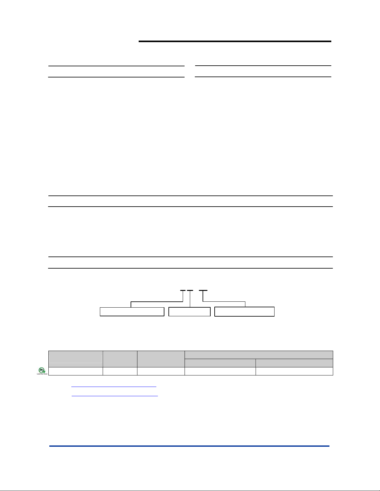
AP5004 S G - 13
With built-in power NMOS, a step-down switching regulator is
easy to be built by adding a coil, capacitors and a diode.
The high efficiency, low standby current, high input voltage (32V)
and output current (2.5A) combining with small SOP-8L package
give AP5004 unprecedented advantage in high power system
applications.
Package
S : SOP-8L
Lead Free
G : Green
Packing
13 : Tape & Reel
Device
Package
Code
Packaging
(Note 2)
Quantity Part Number Suffix
13” Tape and Reel
AP5004SG-13 S SOP-8L 2500/Tape & Reel -13
Notes: 1. EU Directive 2002/95/EC (RoHS). All applicable RoHS exemptions applied. Please visit our website at
http://www.diodes.com/products/lead_free.html
2. Pad layout as shown on Diodes Inc. suggested pad layout document AP02001, which can be found on our website at
http://www.diodes.com/datasheets/ap02001.pdf
.
.
AP5004 Rev. 4 1 of 9 FEBRUARY 2009
www.diodes.com © Diodes Incorporated

AP5004
PWM CONTROL 2.5A STE P -DO WN CONVERTER
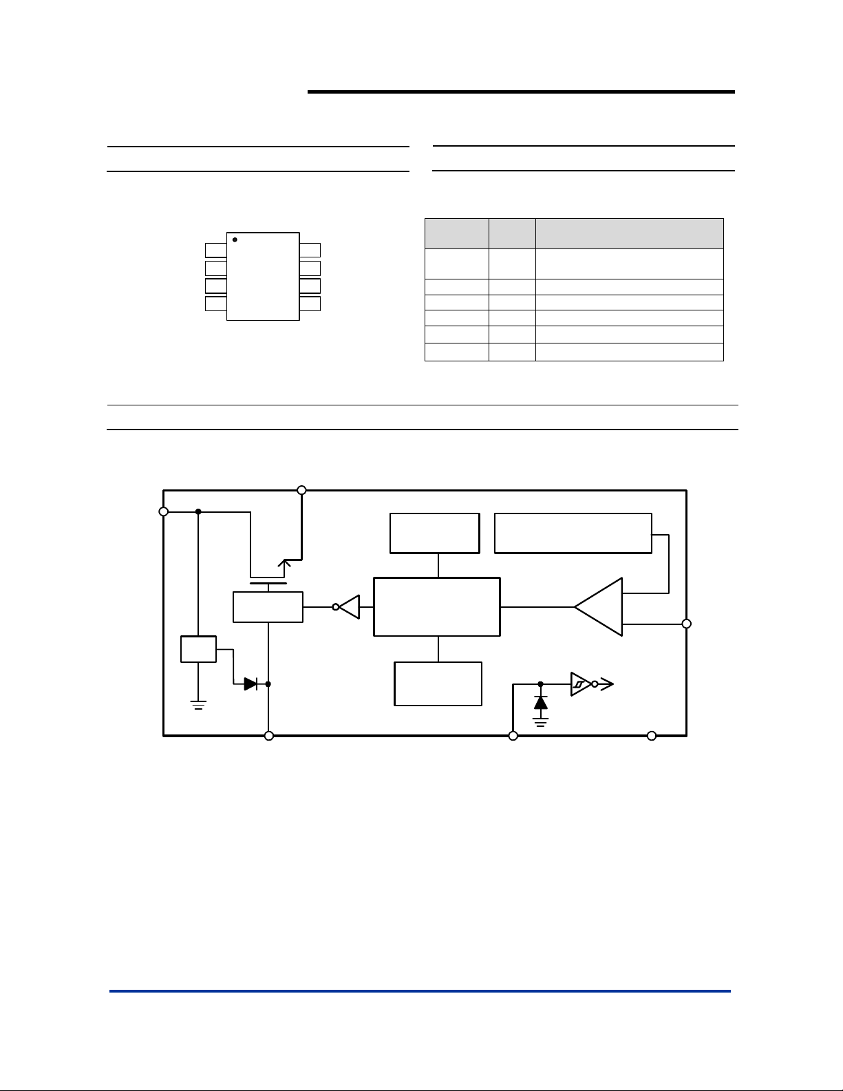
Pin Assignments
(Top View )
1
EN
2
FB
Vboost
Output
3
AP5004
SOP-8L
Block Diagram
Vcc
8
7
6
54
Output
GND
GND
Vcc
Vcc
Pin Descriptions
Pin
Name
EN 1
FB 2 Feedback pin
V
boost
Output 4 Switch output pin
VCC
GND
Oscillation
Circuit
Pin # Description
H: Normal operation
L: Step-down operation stopped
3 High-side gate driver boost pin
5、6
Signal VCC
7、8
GND pin
Reference Voltage
+
-
FB
Driver
PWM -Switched
Control Circuit
VL
Thermal
Shutdown
Vboost
AP5004 Rev. 4 2 of 9 FEBRUARY 2009
www.diodes.com © Diodes Incorporated
V
EN
GNDEN

AP5004
PWM CONTROL 2.5A STE P -DO WN CONVERTER
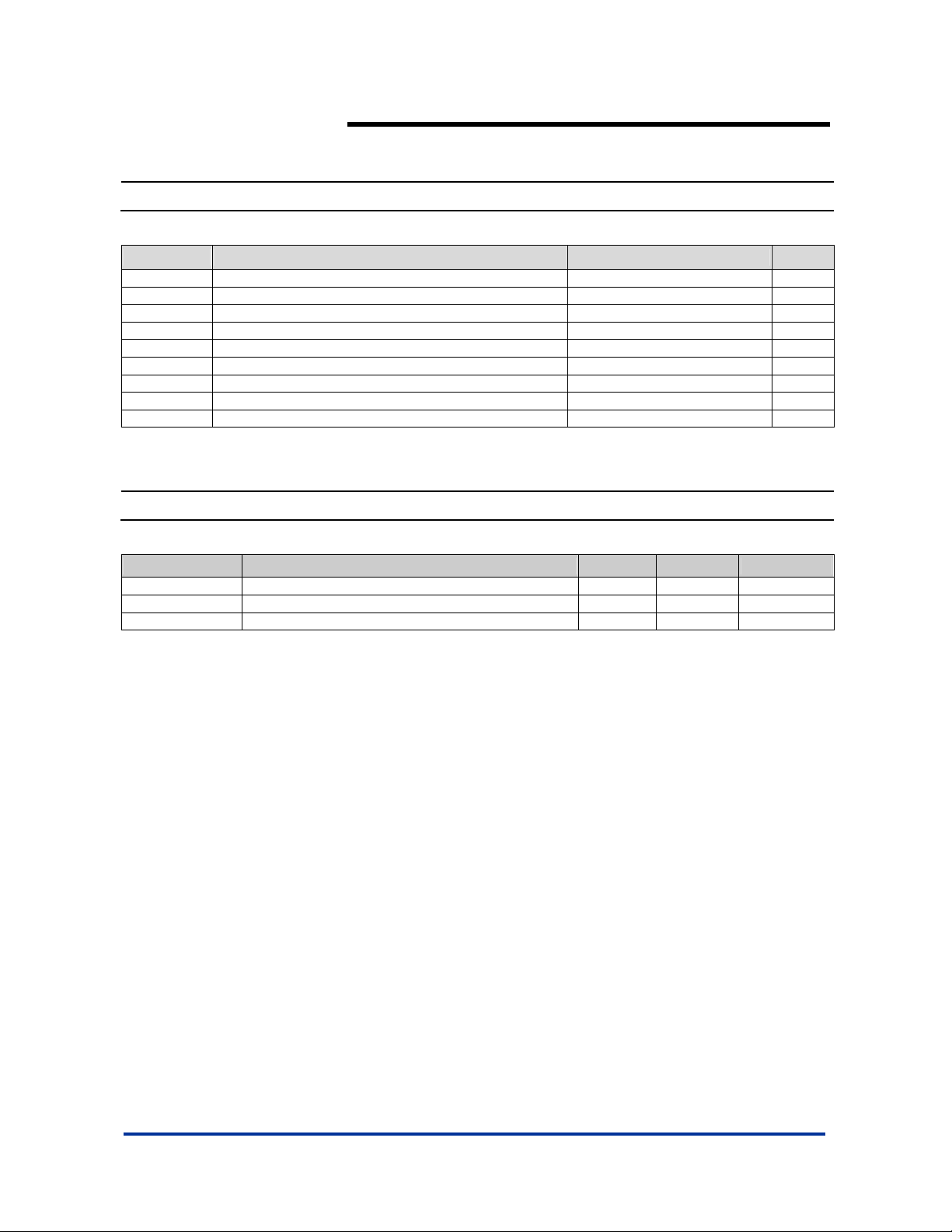
Absolute Maximum Ratings
Symbol Parameter Rating Unit
ESD HBM Human Body Model ESD Protection 1.8 KV
ESD MM Machine Model ESD Protection 550 V
VCC VCC Pin Voltage VSS - 0.3 to VSS + 35 V
VFB V
VEN EN Pi n Voltage VSS - 0.3 to V
V
V
boost
V
Switch Pin Voltage VSS - 0.3 to V
OUTPUT
TJ Operating Junction Temperature Range -10 to +125
T
Storage Temperature Range -40 to +150
ST
Caution: The absolute maximum ratings are rated values exceeding which the product could suffer physical damage. These values must therefore not be
exceeded under any conditions.
Recommended Operating Conditions
Symbol Parameter Min Max Unit
VIN Input Voltage 10 32 V
I
Output Current 0 2.5 A
OUT
TA Operating Ambient Temperature -10 85
Pin Voltage VSS - 0.3 to VCC V
OUT
+ 0.3 V
CC
Pin Voltage V
boost
+ 7V V
OUTPUT
+ 0.3 V
CC
o
C
o
C
o
C
AP5004 Rev. 4 3 of 9 FEBRUARY 2009
www.diodes.com © Diodes Incorporated
 Loading...