diodes incorporated AP358 Service Manual
AP358
LOW POWER DUAL OPE RAT IO NA L AM PL I FI E RS
Features
• Internally frequency compensated for unity gain
• Large dc voltage gain: 100 dB
• Very low supply current drain (500μA)-essentially
independent of supply voltage
• Wide bandwidth (unity gain): 1 MHz (temperature
compensated)
• Input common-mode voltage range includes gr ound
• Differential input voltage range equal to the power
supply voltage
• Low input offset voltage: 2mV
• Wide power supply range:
Single supply: 3V to 32V
Or dual supplies: ±1.5V to ±16V
• Large output voltage swing: 0V to V
• SOP-8L and PDIP-8L packages (Note 1)
• SOP-8L: Available in “Green” Molding Compound
(No Br, Sb)
• Lead Free Finish/RoHS Compliant (Note 2)
+
- 1.5V
Advantages
• Eliminate the need for dual supplies
• Compatible with all forms of logic
• Two internally compensated op amps
• Low power drain suitable for battery operation
• Allows direct sensing near GND and V
OUT
General Description
The AP358 series consists of two independent, high gain,
internally frequency compensated operational amplifiers which
were designed specifically to operate from a single power supply
over a wide range of voltages. Operation from split power
supplies is also possible and the low power supply current drain
is independent of the magnitude of the power supply voltage.
Application areas include transducer amplifiers, dc gain blocks
and all the conventional op amp circuits which now can be more
easily implemented in single power supply systems. For example,
the AP358 series can be directly operated off of the standard +5V
power supply vo ltage which is used in di gital systems and will
easily provide the required interface electronics without requiring
the additional ±15V power supply.
also goes to GND
Ordering Information
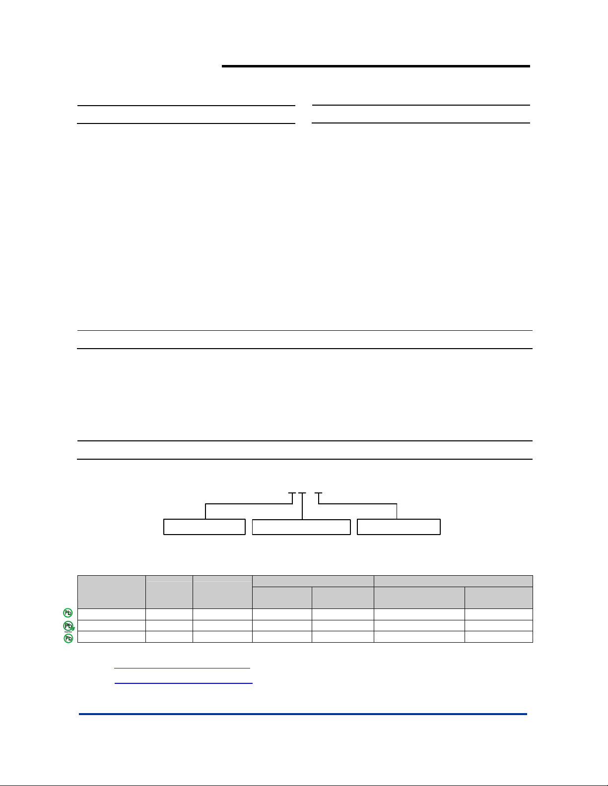
AP 3 5 8 X X - X
Package
S : SOP-8L
N : PDIP-8L
Lead Free
L : Lead Free (Note 1)
G : Green
Device
AP358SL-13 S SOP-8L NA NA 2500/Tape & Reel -13
Lead-free
Package
Code
Packaging
(Note 3)
Quantity
Tube 13” Tape and Reel
Part Number
Suffix
AP358SG-13 S SOP-8L NA NA 2500/Tape & Reel -13
AP358NL-U N PDIP-8L 60 - U NA NA
Lead-free
Notes: 1. PDIP-8L is available in “Lead Free” product only.
2. EU Directive 2002/95/EC (RoHS). All applicable RoHS exemptions applied. Please visit ou r website at
http://www.diodes.com/products/lead_free.html
3. Pad layout as shown on Diodes Inc. suggested pad layout document AP02001, which can be found on our website at
http://www.diodes.com/datasheets/ap02001.pdf
.
.
AP358 Rev. 5 1 of 17 FEBRUARY 2009
www.diodes.com © Diodes Incorporated
Packing
U : Tube
13 : Tape & Reel
Quantity
Part Number
Suffix
AP358
LOW POWER DUAL OPE RAT IO NA L AM PL I FI E RS
Unique Characteristics
• In the linear mode the input common-mode voltage range includes ground and the output voltage can also swing to ground,
even though operated from only a single power supply voltage.
• The unity gain cross frequency is temperature compensated.
• The input bias current is also temperature compensate
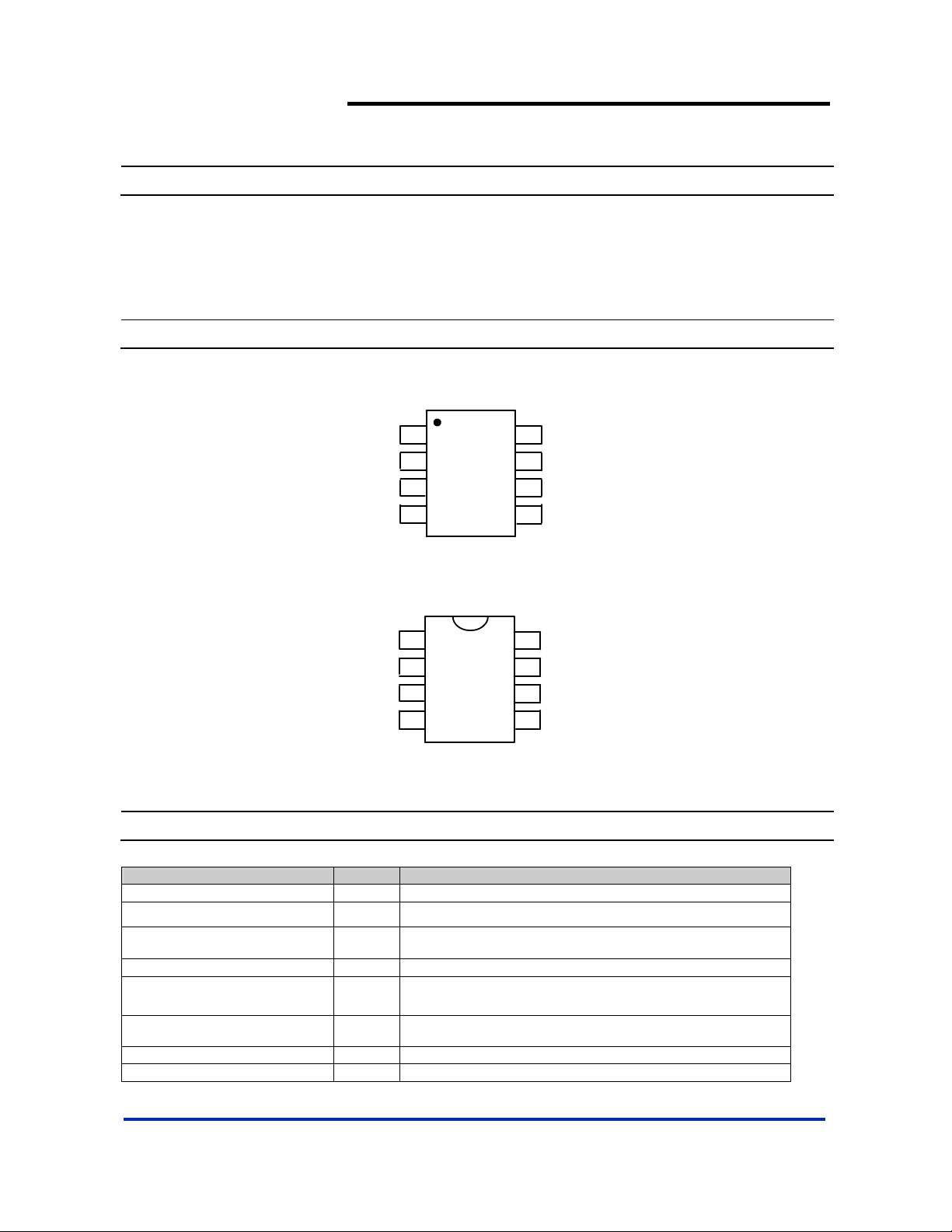
Pin Assignment
( Top View )
OUTPUT 1
INVERTING INPUT 1
NON-INVERTING INPUT 1
GND
1
2
AP358
3
45
V
8
OUTPUT 2
7
INVERTING INPUT 2
6
NON-INVERTING INPUT 2
SOP-8L
( Top View )
OUTPUT 1
INVERTING INPUT 1
NON-INVERTING INPUT 1
GND
1
2
AP358
3
45
V
8
OUTPUT 2
7
INVERTING INPUT 2
6
NON-INVERTING INPUT 2
PDIP-8L
Pin Descriptions
Pin Name Pin # Description
OUTPUT 1 1 Channel 1 Output
INVERTING INPUT 1 2 Channel 1 Inverting Input
+
+
NON-INVERTING INPUT 1 3 Channel 1 Non-inverting Input
GND 4 Ground
NON-INVERTING INPUT 2 5 Channel 2 Non-inverting Input
INVERTING INPUT 2 6 Channel 2 Inverting Input
OUTPUT 2 7 Channel 2 Output
V+ 8 Chip Supply Voltage
AP358 Rev. 5 2 of 17 FEBRUARY 2009
www.diodes.com © Diodes Incorporated
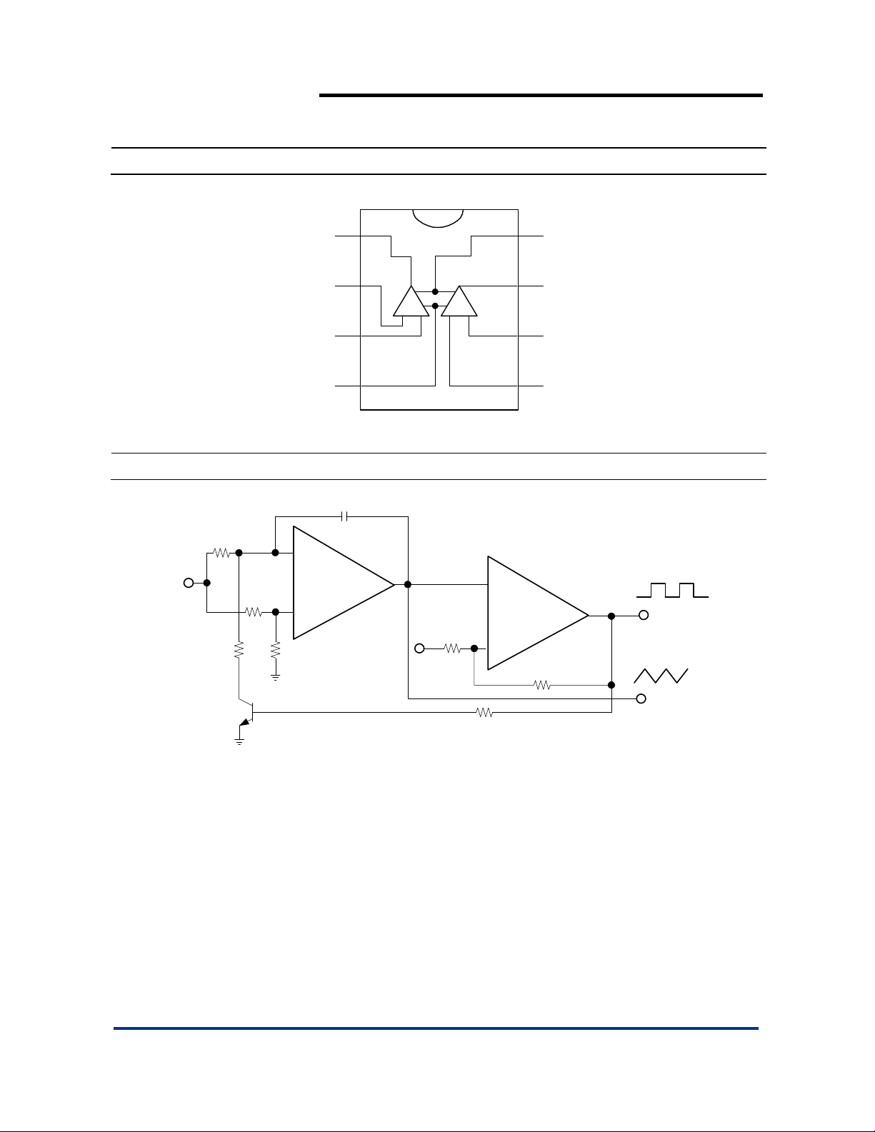
Block Diagram
AP358
LOW POWER DUAL OPE RAT IO NA L AM PL I FI E RS
GND
1
2
AB
3
4
OUTPUT 1
INVERTING INPUT 1
NON-INVERTING INPUT 1
Voltage Controlled Oscillator (VCO)
+V
R
100K
*
C
51K
R/2
51K
0.05μF
-
1/2 AP358
+
V
51K
+-+-
-
+
/2
51K
1/2 AP358
+
8
+
V
7
OUTPUT 2
6
INVERTING INPUT 2
5
NON-INVERTING INPUT 2
100K
OUTPUT1
OUTPUT2
10K
AP358 Rev. 5 3 of 17 FEBRUARY 2009
www.diodes.com © Diodes Incorporated
AP358
LOW POWER DUAL OPE RAT IO NA L AM PL I FI E RS
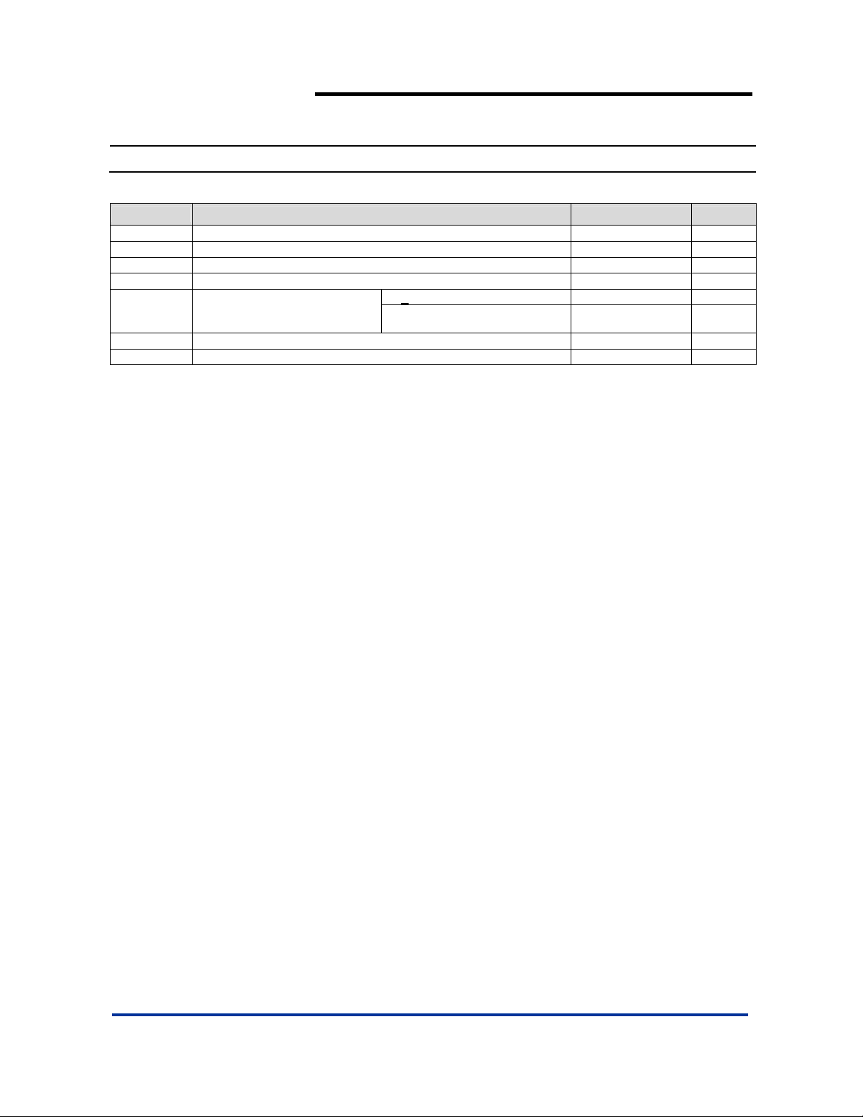
Absolute Maximum Ratings
Symbol Parameter Rating Unit
VCC Supply voltage 32 V
VIN Input Voltage -0.3 to +32 V
PD Power Dissipation (Note 4)
TOP Operating Temperature Range 0 to +70
TST Storage Temperature Range -65 to +150
Notes: 4. For operating at high temperatures, the AP358 must be derated based on a +125°C maximum junction temperature and a
thermal resistance of 120°C/W for DIP and 189°C/W for Small Outline package, which applies for the device soldered in a
printed circuit board, operating in a still air ambient. The dissipation is the total of both amplifiers—use external resistors,
where possible, to allow the amplifier to saturate or to reduce the power which is dissipated in the integrated circuit.
to ground, the maximum output current is approximately 40mA independent of the magnitude of V
voltage in excess of +15V, continuous short-circuits can exceed the power dissipation ratings and cause eventual
destruction. Destructive dissipation can result from simultaneous shorts on all amplifiers.
6. This input current will only exist when the voltage at any of the input leads is driven negative. It is due to the collector-base
junction of the input PNP transistors becoming forward biased and thereby acting as input diode clamps. In addition to this
diode action, there is also lateral NPN parasitic transistor action on the IC chip. This transistor action can cause the output
voltages of the op amps to go to the V
driven negative. This is not destructive and normal output states will re-establish when the input voltage, which was
negative, again returns to a value greater than -0.3V (at 25°C).
Differential Input Voltage 32 V
600 mW
40 mA
Output Short-Circuit to GND
(One Amplifier)
5. Short circuits from the output to V
(Note 5)
+
+
< 15V and TA=25oC Continuous
V
Input Current (VIN < -0.3V)
(Note 6)
can cause excessive heating and eventual destruction. When considering short circuits
+
voltage level (or to ground for a large overdrive) for the time duration that an input is
+
. At values of supply
o
C
o
C
AP358 Rev. 5 4 of 17 FEBRUARY 2009
www.diodes.com © Diodes Incorporated
AP358
LOW POWER DUAL OPE RAT IO NA L AM PL I FI E RS
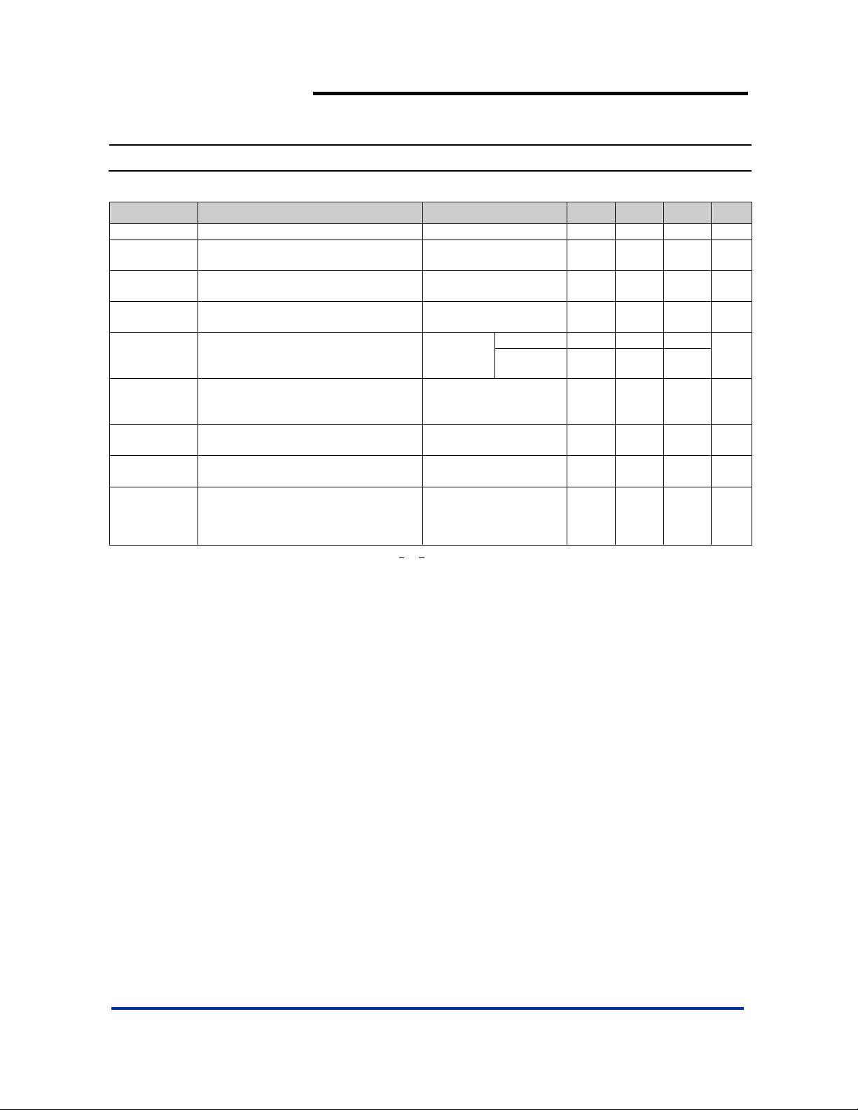
Electrical Characteristics (T
= 25oC, V+ = +5.0V, unless otherwise stated) (Note 7)
A
Symbol Parameter Conditions Min Typ. Max Unit
VIO Input Offset Voltage TA= 25oC, (Note 8) - 2 7 mV
or I
IB Input Bias Current
IIO Input Offset Current
V
Inpu t Co m mo n- Mode Voltage Rang e
ICM
IS
Supply Current
Over Full Temperature Range
AV Large Signal Voltage Gain
CMRR Common-Mode Rejection Ratio
PSRR Power Supply Rejection Ratio
I
IN(+)
V
CM
I
IN(+)
= 25°C
T
A
+
V
= 30V, (Note 10)
T
= 25°C
A
= ∞ on
R
L
All Op
Amps
+
= 15V, TA = 25°C,
V
R
> 2kΩ,
L
(For V
T
= 25°C, V
A
+
-1.5V
V
+
V
= 5V to 30V,
= 25°C
T
A
, TA = 25°C,
IN(−)
= 0V, (Note 9)
- I
IN(−),VCM
= 0V,
+
V
V+ = 5V - 0.5 1.2
= 1V to 11V)
O
CM
- 45 250 nA
- 5 50 nA
0 - V
+
= 30V - 1 2
25 100 - V/mV
= 0V to
65 85 - dB
65 100 - dB
-1.5 V
mA
f = 1KHz to 20 KHz,
= 25°C
T
Amplifier-to-Amplifier Coupling
Notes: 7. The AP358 temperature specifications are limited to 0°C < TA < +70°C.
8. V
9. The direction of the input current is out of the IC due to the PNP input stage. This current is essentially constant,
independent of the state of the output so no loading change exists on the input lines.
25°C). The upper end of the common-mode voltage range is V
without damage, independent of the magnitude of V
external parts. This typically can be detected as this type of capacitance increases at higher frequencies.
≅ 1.4V, R
O
10. The input common-mode voltage of either input signal voltage should not be allowed to go negative by more than 0.3V (at
11. Due to proximity of external components, insure that coupling is not originating via stray capacitance between these
= 0Ω with V+ from 5V to 30V; and over the full input common-mode range (0V to V+ -1.5V) at 25°C.
S
+
.
A
(Input Referred),
(Note 11)
+
-1.5V (at 25°C), but either or both inputs can go to +32V
- -120 - dB
AP358 Rev. 5 5 of 17 FEBRUARY 2009
www.diodes.com © Diodes Incorporated
AP358
LOW POWER DUAL OPE RAT IO NA L AM PL I FI E RS
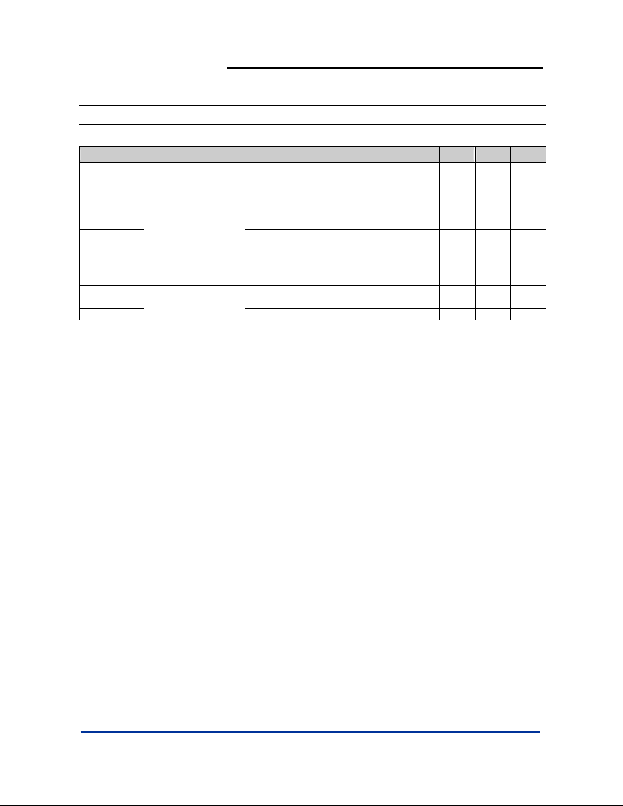
Electrical Characteristics (Continued) (V
Symbol Parameter Conditions Min Typ. Max Unit
I
SINK
Output Current
I
Source
SOURCE
ISC Short Circuit to Ground
VOH
Output Vol tage Swing
VOL (V+=5V) RL= 10kΩ, TA= 25oC - 5 20 mV
Notes: 5. Short circuits from the output to V+ can cause excessive heating and eventual destruction. When considering short circuits
to ground, the maximum output current is approximately 40mA independent of the magnitude of V
voltage in excess of +15V, continuous short-circuits can exceed the power dissipation ratings and cause eventual
destruction. Destructive dissipation can result from simultaneous shorts on all amplifiers.
Sink
(V+=30V)
+
= +5.0V, unless otherwise stated) (Note 5)
-
V
= 1V, V
IN
+
V
= 15V, VO = 2V, T
= 25°C
-
V
= 1V, V
IN
+
= 15V, VO = 200mV,
V
= 25°C
T
A
+
= 1V, V
V
IN
+
V
= 15V, VO = 2V,
= 25°C
T
A
T
= 25°C, (Note 5)
A
+
V
= 15V
= 2kΩ, TA= 25oC 26 - - V
R
L
+
= 0V,
IN
+
= 0V,
IN
-
= 0V,
IN
10 20 - mA
A
20 70 - μA
20 40 - mA
- 40 60 mA
RL= 10kΩ, TA= 25oC 27 28 - V
+
. At values of supply
AP358 Rev. 5 6 of 17 FEBRUARY 2009
www.diodes.com © Diodes Incorporated
 Loading...