diodes incorporated AP1117 Service Manual

查询AP1117D15G-13供应商
Features
• 1.4V Maximum Dropout at Full Load Current
• Fast Transient Response
• Output Current Limiting
• Built-in Thermal Shutdown
• Good Noise Rejection
• 3-Terminal Adjustable or Fixed 1.5V, 1.8V, 2.5V, 3.3V,
• SOT223-3L, TO252-3L, SOT89-3L, TO263-3L and
• SOT223-3L and TO252-3L: Available in “Green”
• Lead Free Finish/RoHS Compliant (Note 1)
Applications
• PC Peripheral
• Communication
5.0V
TO220-3L Packages
Molding Compound (No Br, Sb)
AP1117
1A LOW DROPOUT POSITIVE ADJUSTABLE OR
FIXED-MODE REGULATOR
General Description
AP1117 is a low dropout positive adjustable or fixed-mode
regulator with 1A output current capability. The product is voltage
specifically designed to provide well-regulated supply for low IC
applications such as high-speed bus termination and low current
3.3V logic supply. AP1117 is also well suited for other
applications such as VGA cards. AP1117 is guaranteed to have
lower than 1.4V dropout at full load current making it ideal to
provide well-regulated outputs of 1.25 to 5.0 with 6.4V to 18V
input supply. AP1117 is available in both commercial and
industrial temperature grade.
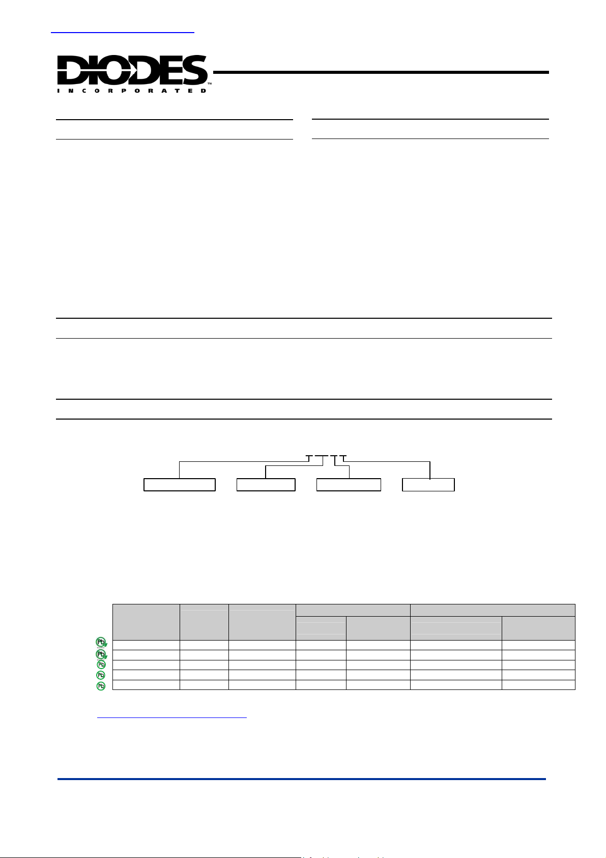
Ordering Information
XX X X
A P 1 1 1 7
Package
D : TO252-3L
E : SOT223-3L
K : TO263-3L
T : TO220-3L
Y : SOT89-3L
Blank: Adj
15: 1.5V
18: 1.8V
25: 2.5V
33: 3.3V
50: 5.0V
Note: 1. Green is only for SOT223-3L and TO252-3L.
2. RoHS revision 13.2.2003. Glass and High Temperature Solder Exemptions Applied, see EU Directive Annex Notes 5 and 7.
Device
AP1117D D TO252-3L 80 -U 2500/Tape & Reel -13
AP1117E E SOT223-3L 75 -U 2500/Tape & Reel -13
Lead-free
Lead-free
Note: 3. Pad layout as shown on Diodes Inc. suggested pad layout document AP02001, which can be found on our website at
http://www.diodes.com/datasheets/ap02001.pdf.
Lead-free
AP1117K K TO263-3L 50 -U 800/Tape & Reel -13
AP1117T T TO220-3L 50 -U NA NA
AP1117Y Y SOT89-3L NA NA 2500/Tape & Reel -13
Package
Code
Packaging
(Note 3)
X
Lead Free
L : Lead Free
:
Green (Note 1)
G
Quantity
PackingVout
-U :
Tube
:
Taping
-13
Tube 13” Tape and Reel
Part Number
Suffix
Quantity
Part Number
Suffix
AP1117 Rev. 6 1 of 11 MARCH 2007
www.diodes.com © Diodes Incorporated

AP1117
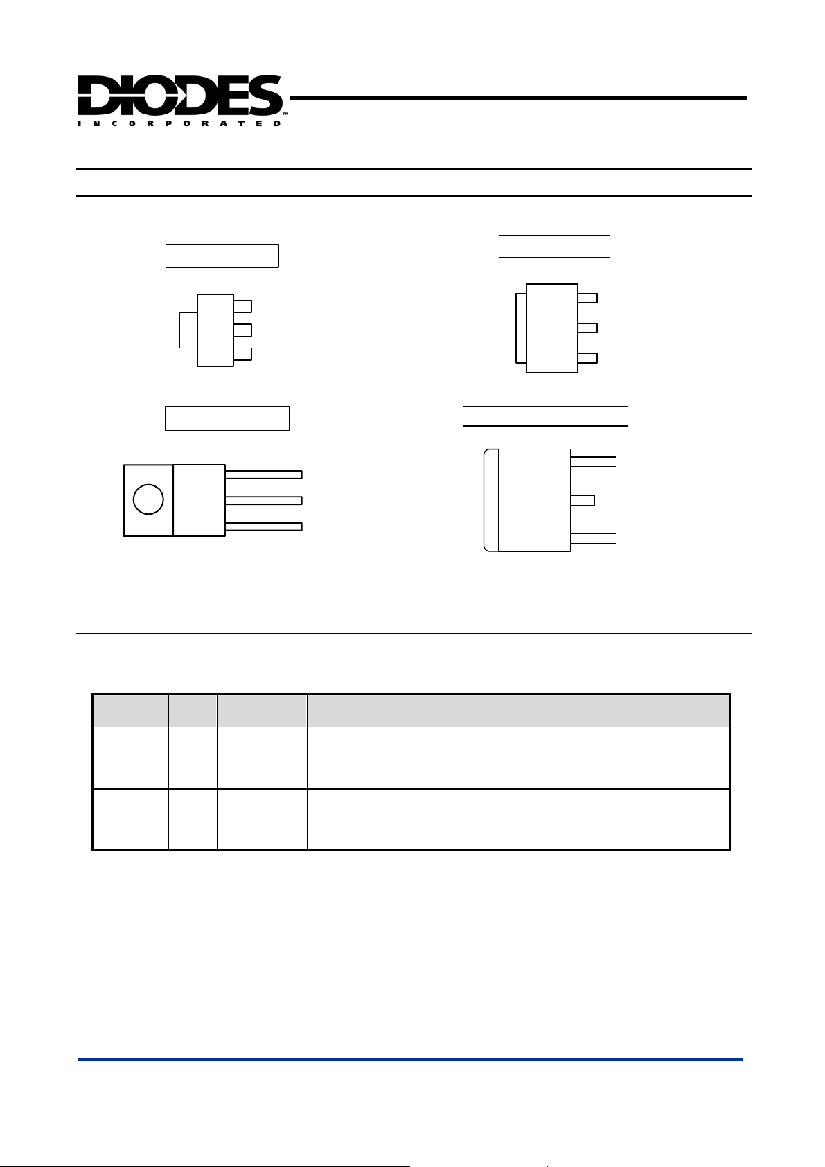
Pin Assignments
SOT89-3L
3
2
1
Tab is Vout
TO220-3L
FRONT VIEW
3
2
1
Tab is V
Vin
Vout
Adj (GND)
out
V
in
V
out
Adj (GND)
1A LOW DROPOUT POSITIVE ADJUSTABLE OR
FIXED-MODE REGULATOR
SOT223-3L
( Top View )
3
Vin
Vout
2
1
Adj (GND)
TO252-3L / TO263-3L
Tab is Vout
( Top View )
3
2
1
Tab is Vout
Vin
Vout
Adj (GND)
Pin Descriptions
NAME I/O PIN # FUNCTION
Adj (GND) I 1
V
Vin
out
O 2
I 3
A resistor divider from this pin to the V
(Ground only for Fixed-Mode).
The output of the regulator. A minimum of 10uF capacitor (0.15Ω ≤ ESR ≤ 20Ω)
must be connected from this pin to ground to insure stability.
The input pin of regulator. Typically a large storage capacitor (0.15Ω ≤ ESR ≤ 20Ω)
is connected from this pin to ground to insure that the input voltage does not sag
below the minimum dropout voltage during the load transient response. This pin
must always be 1.3V higher than V
pin and ground sets the output voltage
out
in order for the device to regulate properly.
out
AP1117 Rev. 6 2 of 11 MARCH 2007
www.diodes.com © Diodes Incorporated

AP1117
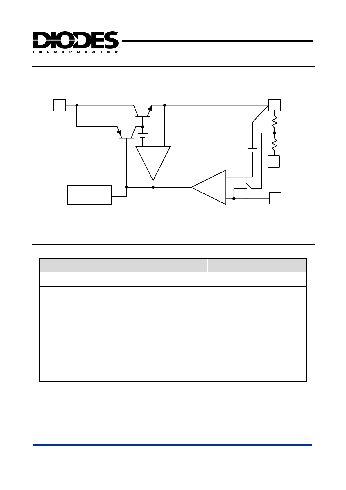
Block Diagram
3
V
in
Thermal
Shutdown
1A LOW DROPOUT POSITIVE ADJUSTABLE OR
FIXED-MODE REGULATOR
2
V
out
+
+
-
1.25V
CURRENT
LIMIT
+
-
+
1
GND
(FIXED)
1
Adj
Absolute Maximum Ratings
Symbol Parameter Rating Unit
Vin DC Supply Voltage -0.3 to 18 V
TOP
TMJ Maximum Junction Temperature 150
PD
TST Storage Temperature -65 to +150
Note: 4. AP1117 contains an internal thermal limiting circuit that is designed to protect the regulator in the event that the maximum junction temperature
exceeded. When activated, typically at 150°C, the regulator output switches off and then back on as the die cools.
AP1117 Rev. 6 3 of 11 MARCH 2007
www.diodes.com © Diodes Incorporated
Operating Junction Temperature Range
(Commercial Grade)
Power Dissipation
SOT89-3L
SOT223-3L
TO220-3L
TO252-3L
TO263-3L
0 to +125
Internally limited by
maximum junction
temperature
of 150 oC (Note 4)
o
C
oC
mW
o
C

θ
θ
AP1117
1A LOW DROPOUT POSITIVE ADJUSTABLE OR
FIXED-MODE REGULATOR
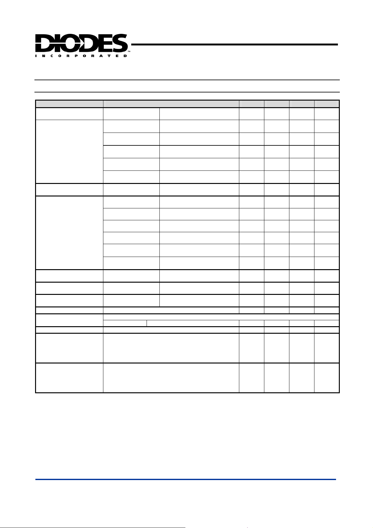
Electrical Characteristics (Under Operating Conditions)
PARAMETER CONDITIONS MIN TYP MAX UNIT
= 25oC, (VIN-
T
Reference Voltage AP1117-ADJ
AP1117-1.5
AP1117-1.8
Output Voltage
AP1117-2.5
AP1117-3.3
AP1117-5.0
Line Regulation AP1117-XXX
AP1117-ADJ
AP1117-1.5
AP1117-1.8
Load Regulation
AP1117-2.5
AP1117-3.3
AP1117-5.0
Dropout Voltage
IN-VOUT
)
(V
Current Limit
Minimum Load Current
(Note 7)
AP1117-ADJ/1.5/1.8
/2.5/3.3/5.0
AP1117-ADJ/1.5/1.8
/2.5/3.3/5.0
AP1117-XXX
A
= 10mA
I
O
= 10mA, TA = 25oC,
I
OUT
≦12V
3V≦V
IN
= 10mA, TA = 25oC,
I
OUT
3.3V≦V
IN
= 10mA, TA = 25oC,
I
OUT
≦12V
4V≦V
IN
= 10mA, TA = 25oC,
I
OUT
4.8V≦V
IN
= 10mA, TA = 25oC,
I
OUT
6.5V≦V
IN
I
= 10mA,V
O
= 25oC
T
A
=3.3V,Vadj=0,0mA<Io<1A,
V
IN
= 25oC (Note 5, 6)
T
A
= 3V, 0mA<Io<1A,
V
IN
= 25oC (Note 5, 6)
T
A
= 3.3V, 0mA<Io<1A,
V
IN
= 25oC (Note 5, 6)
T
A
= 4V, 0mA<Io<1A,
V
IN
= 25oC (Note 5, 6)
T
A
V
= 5V, 0≦I
IN
= 25oC (Note 5, 6)
T
A
V
= 8V, 0≦I
IN
= 25oC (Note 5, 6)
T
A
= 1A, ∆V
I
OUT
(V
0
) = 5V 1. 1 A
IN-VOUT
o
C≦Tj≦125oC
Thermal Regulation TA = 25oC, 30ms pulse 0.008 0.04 %/W
Ripple Rejection
F = 180Hz, C
AP1117-XXX V
= 25uF Tantalum, I
OUT
= V
IN
OUT
+3V 60 70 dB
Temperature Stability IO = 10mA 0.5 %
SOT223-3L: Control Circuitry/Power Transistor (Note 8)
Thermal Resistance
JA
Junction-to-Ambient
TO252-3L: Control Circuitry/Power Transistor (Note 9)
SOT89-3L: Control Circuitry/Power Transistor (Note 10)
TO220-3L: Control Circuitry/Power Transistor (Note 11)
TO263-3L: Control Circuitry/Power Transistor (Note 12)
SOT223-3L: Control Circuitry/Power Transistor (Note 8)
Thermal Resistance
JC
Junction-to-Case
TO252-3L: Control Circuitry/Power Transistor (Note 9)
SOT89-3L: Control Circuitry/Power Transistor (Note 10)
TO220-3L: Control Circuitry/Power Transistor (Note 11)
TO263-3L: Control Circuitry/Power Transistor (Note 12)
Notes: 5. See thermal regulation specifications for changes in output voltage due to heating effects. Line and load regulation are measured at a constant
6. Line and load regulation are guaranteed up to the maximum power dissipation of 15W. Power dissipation is determined by the difference
7. Quiescent current is defined as the minimum output current required in maintaining regulation. At 12V input/output differential the
device is guaranteed to regulate if the output current is greater than 10mA.
8. Test condition for SOT223: Ta=27°C, no air flow, 2 oz copper, 5mmx5mm pad.
9. Test condition for TO252: Ta=27°C, no air flow, 2 oz copper, 5mmx5mm pad.
10. Test condition for SOT89-3L: no air flow, no heat sink.
11. Test condition for TO220-3L: with copper area of approximately 3in
junction temperature by low duty cycle pulse testing. Load regulation is measured at the output lead = 1/18” from the package.
between input and output differential and the output current. Guaranteed maximum power dissipation will not be available over the full
input/output range.
12. Test condition for TO263-3L: with copper area of approximately 2cmX2cm, 1 oz, no air flow.
) = 1.5V
OUT
1.225 1.250 1.275 V
1.470 1.500 1.530 V
≦12V
1.764 1.800 1.836 V
2.450 2.500 2.550 V
≦12V
≦12V
+1.5V<VIN<12V,
OUT
3.235 3.300 3.365 V
4.900 5.000 5.100 V
0.2 %
1 %
18 15 mV
15 18 mV
20 25 mV
≦1A,
OUT
OUT
OUT
≦1A,
= 0.1%V
OUT
26 33 mV
40 50 mV
1.3 1.4 V
5 10 mA
= 1A
OUT
107
182
31.35
73
O
C/W
95
12
16
42
5.25
O
C/W
19
2
, 1 oz, no air flow.
AP1117 Rev. 6 4 of 11 MARCH 2007
www.diodes.com © Diodes Incorporated
 Loading...