diodes incorporated 74LVC1G32 Service Manual

74LVC1G32
A
A
(
)
SINGLE 2 INPUT POSITIVE OR GATE
Description
The 74LVC1G32 is a single 2-input positive OR gate with a
standard push-pull output. The device is designed for
operation with a power supply range of 1.65V to 5.5V. The
inputs are tolerant to 5.5V allowing this device to be used in a
mixed voltage environment. The device is fully specified for
partial power down applications using I
disables the output preventing damaging current backflow
when the device is powered down.
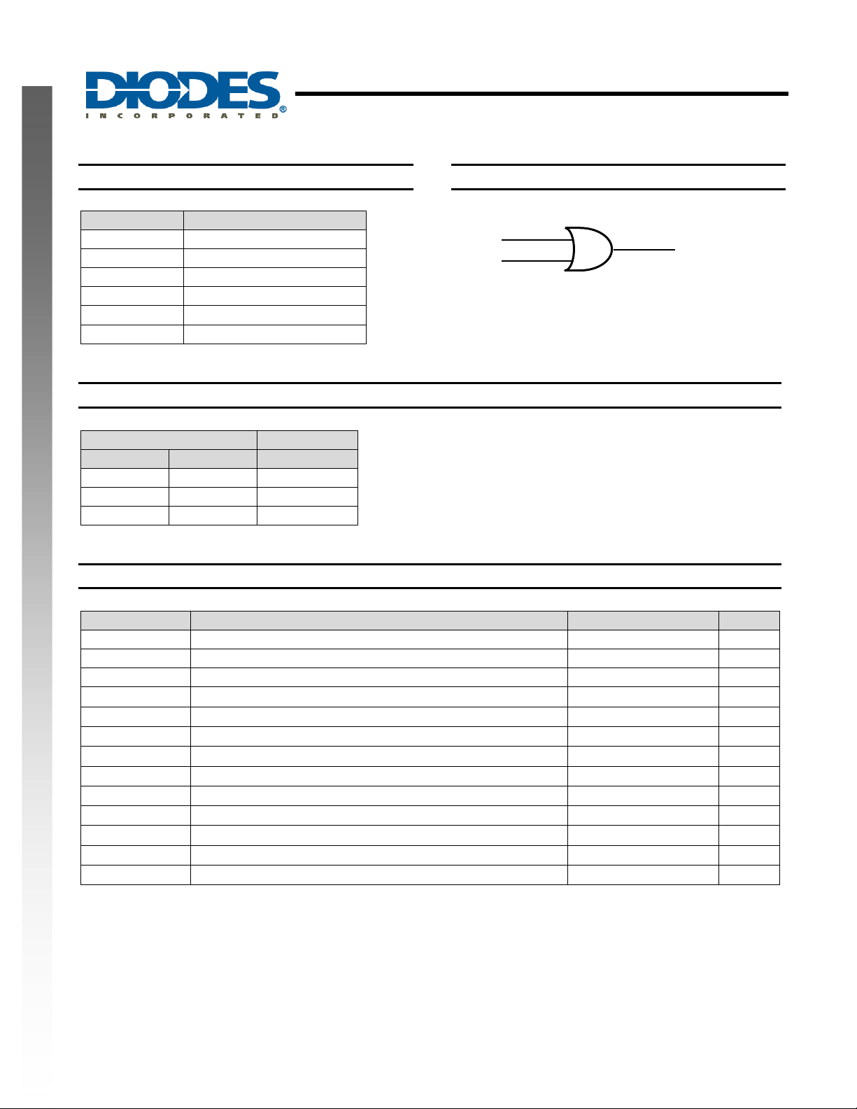
The gate performs the positive Boolean function:
Y += or B
B
Y •=
OFF
. The I
Features
• Wide Supply Voltage Range from 1.65 to 5.5V
NEW PRODUCT
• ± 24mA Output Drive at 3.3V
• CMOS low power consumption
• I
• Inputs accept up to 5.5V
• ESD Protection Tested per JESD 22
• Latch-Up Exceeds 100mA per JESD 78, Class II
• Range of Package Options
• Direct Interface with TTL Levels
• All packages Assembled with “Green” Molding
• Lead Free Finish/ RoHS Compliant (Note 1)
Supports Partial-Power-Down Mode Operation
OFF
o Exceeds 200-V Machine Model (A115-A)
o Exceeds 2000-V Human Body Model (A114-A)
o Exceeds 1000-V Charged Device Model (C101C)
Compound (no Br, Sb)
OFF
circuitry
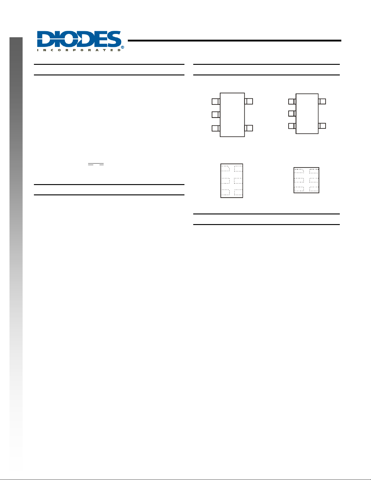
Pin Assignments
A
B
GND
GND
(Top View)
1
2
3
SOT25
(Top View)
136
A
B
5
2
4
DFN1410
V
NC
Y
5
4
CC
V
CC
Y
GND
A
B
GND
Top View
1
2
3
SOT353
(Top View)
1
A
2
B
3
DFN1010
Applications
• Voltage Level Shifting
• General Purpose Logic
• Bus Driver / Repeater
• Power Down Signal Isolation
• General Purpose Logic
• Wide array of products such as:
o PCs, networking, notebooks, netbooks, PDAs
o Tablet Computers, E-readers
o Computer peripherals, hard drives, CD/DVD ROM
o TV, DVD, DVR, set top box
o Cell Phones, Personal Navigation / GPS
o MP3 players ,Cameras, Video Recorders
V
5
CC
4
Y
6
V
CC
5
NC
4
Y
Notes: 1. EU Directive 2002/95/EC (RoHS). All applicable RoHS exemptions applied. Please visit our website at
http://www.diodes.com/products/lead_free.html.
74LVC1G32
Document number: DS32200 Rev. 4 - 2
1 of 10
www.diodes.com
October 2011
© Diodes Incorporated

Pin Descriptions
74LVC1G32
SINGLE 2 INPUT POSITIVE OR GATE
Logic Diagram
Pin Name Description
A Data Input
B Data Input
GND Ground
Y Data Output
VCC
NC No Connection
Supply Voltage
Function Table
Inputs Output
A B Y
NEW PRODUCT
H X H
X H H
L L L
Absolute Maximum Ratings (Note 2)
Symbol Description Rating Unit
ESD HBM Human Body Model ESD Protection 2 KV
ESD CDM Charged Device Model ESD Protection 1 KV
ESD MM Machine Model ESD Protection 200 V
VCC
VI
Vo Voltage applied to output in high impedance or I
Vo
IIK Input Clamp Current VI<0
IOK
IO
I
CC, IGND
TJ
T
STG
Notes: 2. Stresses beyond the absolute maximum may result in immediate failure or reduced reliability. These are stress values and device
operation should be within recommend values.
Supply Voltage Range -0.5 to 6.5 V
Input Voltage Range -0.5 to 6.5 V
Voltage applied to output in high or low state.
Output Clamp Current -50 mA
Continuous output current ±50 mA
Continuous curr ent through VCC or GND
Operating Junction Temperature -40 to 150 °C
Storage Temperature -65 to 150 °C
74LVC1G32
Document number: DS32200 Rev. 4 - 2
OFF
2 of 10
www.diodes.com
state
1
2
-0.5 to 6.5 V
-0.3 to VCC +0.5
4
Y
V
-50 mA
±100 mA
October 2011
© Diodes Incorporated

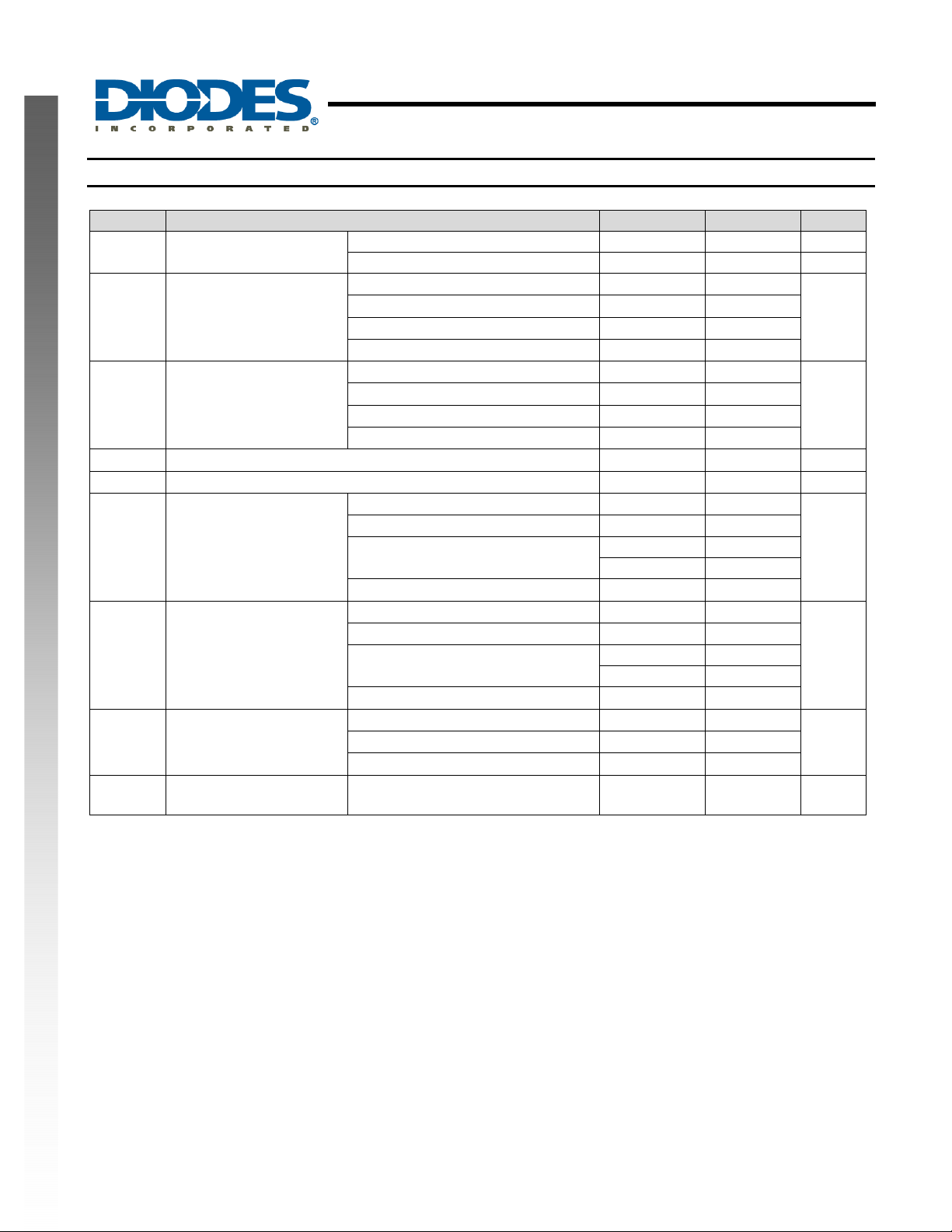
Recommended Operating Conditions (Note 3)
Symbol Parameter Min Max Unit
VCC
V
VIL
VI
VO
NEW PRODUCT
IOH
IOL
Δt/ΔV
TA
Notes: 3. Unused inputs should be held at VCC or Ground.
Operating Voltage
High-level Input Voltage
IH
Low-level input voltage
Input Voltage 0 5.5 V
Output Voltage 0
High-level output current
Low-level output current
Input transition rise or fall
rate
Operating free-air
temperature
Operating 1.65 5.5 V
Data retention only 1.5 V
VCC = 1.65V to 1.95V 0.65 X VCC
VCC = 2.3V to 2.7V
VCC = 3V to 3.6V
VCC = 4.5V to 5.5V 0.7 X VCC
V
= 1.65V to 1.95V
CC
VCC = 2.3V to 2.7V
VCC = 3V to 3.6V
VCC = 4.5V to 5.5V
V
= 1.65V
CC
VCC = 2.3V
VCC = 3V
VCC = 4.5V
= 1.65V
V
CC
VCC = 2.3V
VCC = 3V
VCC = 4.5V
= 1.8V ± 0.15V, 2.5V ± 0.2V
V
CC
VCC = 3.3V ± 0.3V
VCC = 5V ± 0.5V
74LVC1G32
SINGLE 2 INPUT POSITIVE OR GATE
1.7
2
0.7
0.8
-4
-8
-16
-24
-32
4
8
16
24
32
20
10
5
-40 125 ºC
0.35 X VCC
0.3 X VCC
VCC
V
V
V
mA
mA
ns/V
74LVC1G32
Document number: DS32200 Rev. 4 - 2
3 of 10
www.diodes.com
October 2011
© Diodes Incorporated
 Loading...