

Diodes ZXTR2008P5 User Manual
A
f
Product Line o
Diodes Incorporated
Description
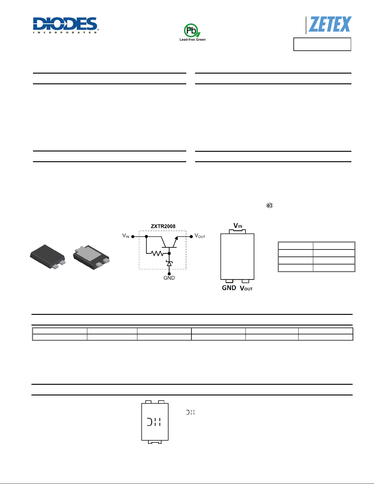
The ZXTR2008P5 monolithically integrates a transistor, Zener diode
and resistor to function as a high voltage linear regulator. The device
regulates with an 8.2V nominal output at 15mA. It is designed for use
in high voltage applications where standard linear regulators cannot
be used. This function is fully integrated into a PowerDI-5 package,
minimizing PCB area and reducing number of components when
compared with a multi-chip discrete solution.
Applications
Supply voltage regulation in:
Networking
Telecom
Power Over Ethernet (PoE)
POWERDI5
Top View
Bottom View
Internal Device
Schematic
ZXTR2008P5
100V INPUT, 8.2V 40mA REGULATOR TRANSISTOR
POWERDI
Features
Series Linear Regulator Using Emitter-Follower Stage
Input Voltage = 12V to 100V
Output Voltage = 8.2V ± 10%
Fully integrated into a PowerDI-5 package
Totally Lead-Free & Fully RoHS compliant (Notes 1 & 2)
Halogen and Antimony Free. “Green” Device (Note 3)
Qualified to AEC-Q101 Standards for High Reliability
Mechanical Data
Case: PowerDI-5
Case Material: Molded Plastic. “Green” Molding Compound.
UL Flammability Rating 94V-0
Moisture Sensitivity: Level 1 per J-STD-020
Terminals: Finish - Matte Tin Plated Leads, Solderable per
MIL-STD-202, Method 208
Weight: 0.100 grams (approximate)
Pin Name Pin Function
VIN Input Supply
GND Power Ground
VOUT Voltage Output
Top View
Pin-Out
®
5
Ordering Information (Note 4)
Product Package Marking Reel size (inches) Tape width (mm) Quantity per reel
ZXTR2008P5-13 PowerDI-5 ZXTR2008 13 16 5,000
Notes: 1. No purposely added lead. Fully EU Directive 2002/95/EC (RoHS) & 2011/65/EU (RoHS 2) compliant.
3. Halogen and Antimony free "Green” products are defined as those which contain <900ppm bromine, <900ppm chlorine (<1500ppm total Br + Cl) and
4. For packaging details, go to our website at http://www.diodes.com/products/packages.html
2. See http://www.diodes.com/quality/lead_free.html for more information about Diodes Incorporated’s definitions of Halogen and Antimony free,"Green"
and Lead-Free.
<1000ppm antimony compounds.
Marking Information
POWERDI is a registered trademark of Diodes Incorporated.
ZXTR2008
DXT790A
YYWWK
ZXTR2008P5
Document number: DS36333 Rev. 1 – 2
ZXTR2008 = Product Type Marking Code
= Manufacturers’ Code Marking
K = Factory Designator
YYWW = Date Code Marking
YY = Last Two Digits of Year (ex: 14 for 2014)
WW = Week code (01 to 53)
1 of 7
www.diodes.com
February 2014
© Diodes Incorporated
A
f
Product Line o
Diodes Incorporated
Absolute Maximum Ratings (Voltage relative to GND, @T
Characteristic Symbol Value Unit
Input Supply Voltage
Continuous Input & Output Current
Peak Pulsed Input & Output Current
Maximum Voltage applied to V
Maximum Current at VIN = 48V (@T
V
OUT
= +25°C, unless otherwise specified.)
A
Characteristic Symbol Value Unit
Continuous Output Current (Note 7)
Pulsed Output Current
(Note 8)
(Note 9) 160
Thermal Characteristics
= +25°C, unless otherwise specified.)
A
V
IN
I
IN, IOUT
I
IM, IOM
OUT(max)
-0.3 to 100 V
450 mA
2 A
14.5 V
I
OUT
I
OM
45 mA
800
ZXTR2008P5
mA
Characteristic Symbol Value Unit
Power Dissipation
Thermal Resistance, Junction to Ambient
(Note 5)
(Note 6) 0.94
(Note 5)
(Note 6) 107
Thermal Resistance, Junction to Lead (Note 10)
Thermal Resistance, Junction to Case (Note 10)
Recommended Operating Junction Temperature Range
Maximum Operating Junction and Storage Temperature Range
P
D
R
θJA
R
θJL
R
θJC
T
J
T
, T
J
STG
1.82
55
20
17.8
-40 to +125
-65 to +150
W
°C/W
°C
ESD Ratings (Note 11)
Characteristics Symbols Value Unit JEDEC Class
Electrostatic Discharge – Human Body Model ESD HBM 4000 V 3A
Electrostatic Discharge – Machine Model ESD MM 400 V C
Notes: 5. For a device mounted with the exposed VIN pad on 50mm x 50mm 1oz copper that is on a single-sided 1.6mm FR4 PCB; device is measured under still
air conditions whilst operating in steady-state.
6. Same as Note 5, except mounted on 15mm x 15mm 1oz copper.
7. Same as Note 5, while operating at V
8. Same as Note 5, except measured with a single pulse width = 100µs and V
9. Same as Note 5, except measured with a single pulse width = 10ms and V
10.
11. Refer to JEDEC specification JESD22-A114 and JESD22-A115
R
= Thermal resistance from junction to solder-point (on the exposed VIN pad).
θJL
R
= Thermal resistance from junction to the top of case.
θJC
= 48V. Refer to Safe Operating Area for other Input Voltages.
IN
IN
= 48V.
IN
= 48V.
.
POWERDI is a registered trademark of Diodes Incorporated.
ZXTR2008P5
Document number: DS36333 Rev. 1 – 2
2 of 7
www.diodes.com
February 2014
© Diodes Incorporated
A
f
Product Line o
Diodes Incorporated
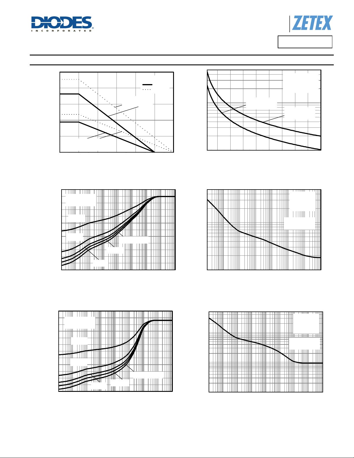
Thermal Characteristics and Derating Information
2.5
T
J
2.0
1.5
50mm x 50mm
= 125°C
= 150°C
1oz Cu
1.0
0.5
15mm x 15mm
1oz Cu
0.0
Max Power Dissipation (W)
0 25 50 75 100 125 150
Ambient temperature (°C)
Continuous Output Current (mA)
Derating Curve
60
50mm x 50mm
50
40
1oz Cu
D=0.5
30
D=0.2
20
Single Pulse
D=0.05
10
D=0.1
0
Thermal Resistance (°C/W)
100µ 1m 10m 100m 1 10 100 1k 10k
Pulse Width (s)
Transient Thermal Impedance
ZXTR2008P5
Steady state D.C.
T
= 25°C
A
T
125°C
J
100
15 mm x 1 5mm
1oz Cu
50mm x 50mm
1oz Cu
10
12 20 30 40 50 60 70 80 90 100
Input Voltage (V)
Safe Operating Area
50
Single Pulse
T
= 25°C
A
T
125°C
J
10
50mm x 50mm
1oz Cu
1
Max Power Dissipation (W)
100µ 1m 10m 100m 1 10 100 1k
Pulse Width (s)
Pulse Power Dissipation
120
100
80
15 mm x 1 5 mm
1oz Cu
D=0.5
50
10
Single Pulse
T
= 25°C
A
T
125°C
J
15mm x 15mm
1oz Cu
60
40
20
0
Thermal Resistance (°C/W)
D=0.2
D=0.1
Single Pulse
D=0.05
100µ 1m 10m 100m 1 10 100 1k 10k
Pulse Width (s)
Transient Thermal Impedance
1
0.1
Max Power Dissipation (W)
100µ 1m 10m 100m 1 10 100 1k 10k
Pulse Width (s)
Pulse Power Dissipation
POWERDI is a registered trademark of Diodes Incorporated.
ZXTR2008P5
Document number: DS36333 Rev. 1 – 2
3 of 7
www.diodes.com
February 2014
© Diodes Incorporated
 Loading...