

Page 1
A
f
y
Product Line o
100V PNP LED DRIVING TRANSISTOR IN SOT223
Features
• BV
• Maximum continuous current I
• h
• Lead Free, RoHS Compliant (Note 1)
• Halogen and Antimony Free "Green" Device (Note 2)
• Qualified to AEC-Q101 Standards for High Reliability
> -100V
CEO
> 100 @ IC = -150mA, VCE = -0.2V
FE
= -1A
C
Applications
• LED TV backlight
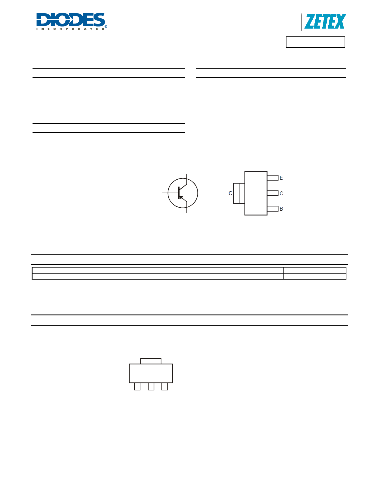
SOT223
B
Top View
Device S
Mechanical Data
• Case: SOT223
• Case material: Molded Plastic. “Green” Molding Compound.
UL Flammability Rating 94V-0
• Moisture Sensitivity: Level 1 per J-STD-020
• Terminals: Matte Tin Finish
• Weight: 0.112 grams (Approximate)
C
E
mbol
Diodes Incorporated
ZXTP4003G
Top View
Pin-Out
Ordering Information
Product Marking Reel size (inches) Tape width (mm) Quantity per reel
ZXTP4003GTA ZXTP4003 7 12 1,000
Notes: 1. No purposefully added lead.
2. “Green” devices, Halogen and Antimony Free, Diodes Inc’s “Green” Policy can be found on our website at http://www.diodes.com
Marking Information
ZXTP
4003
ZXTP4003 = Product type Marking Code
ZXTP4003G
Datasheet Number: DS35459 Rev 1 - 2
1 of 5
www.diodes.com
December 2011
© Diodes Incorporated
Page 2
A
f
Product Line o
Diodes Incorporated
ZXTP4003G
Maximum Ratings @T
Collector-Base Voltage
Collector-Emitter Voltage
Emitter-Base Voltage
Continuous Collector Current
Peak Pulse Current (Note 4)
Base Current
Thermal Characteristics @T
Power Dissipation (Note 3)
Thermal Resistance, Junction to Ambient (Note 3)
Thermal Resistance, Junction to Leads (Note 5)
Operating and Storage Temperature Range
Notes: 3. For a device surface mounted on 25mm X 25mm FR4 PCB with high coverage of single sided 1 oz copper, in still air conditions
4. Measured under pulsed conditions. Pulse width = 300µs. Duty cycle ≤ 2%.
5. Thermal resistance from junction to solder-point (on the exposed collector pad).
= 25°C unless otherwise specified
A
Characteristic Symbol Value Unit
V
CBO
V
CEO
V
EBO
I
C
I
CM
I
B
= 25°C unless otherwise specified
A
Characteristic Symbol Value Unit
P
D
R
θJA
R
θJL
T
J, TSTG
-100 V
-100 V
-7 V
-1 A
-3 A
-500 mA
2 W
62.5
28.75
-55 to +150
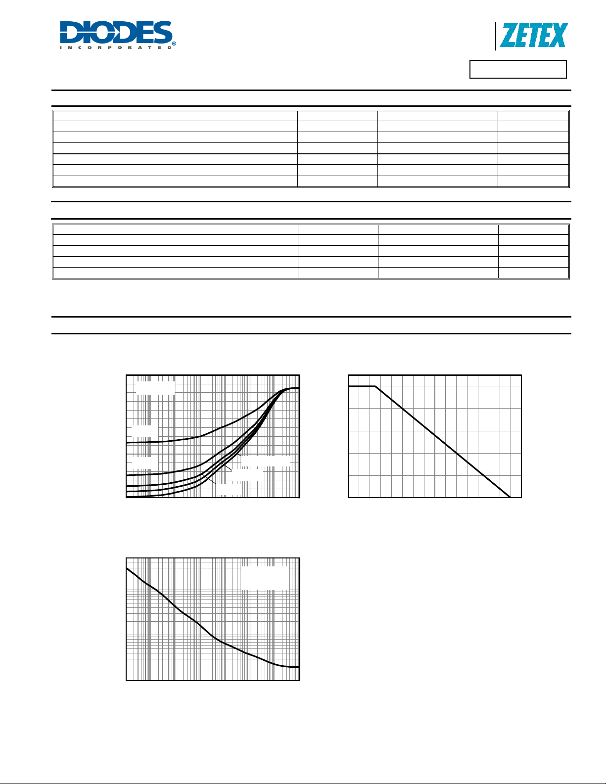
Thermal Characteristics and Derating Information
70
60
50
T
amb
=25°C
2.0
1.6
°C/W
°C/W
°C
40
D=0.5
30
20
D=0.2
10
0
100µ 1m 10m 100m 1 10 100 1k
Thermal Resistance (°C/ W)
Pulse Width (s)
Single Pulse
D=0.05
D=0.1
Transient Thermal Impedance
Single Pulse
T
100
amb
10
Maximum Power (W)
1
100µ 1m 10m 100m 1 10 100 1k
Pulse Width (s)
Pulse Power Dissipation
=25°C
1.2
0.8
0.4
0.0
0 20 40 60 80 100 120 140 160
Max Power Di ssipation (W )
Temperature (°C)
Derating Curve
ZXTP4003G
Datasheet Number: DS35459 Rev 1 - 2
2 of 5
www.diodes.com
December 2011
© Diodes Incorporated
Page 3

A
f
)
(d)
(r
)
(s)
(f)
(s)
(f)
Product Line o
Diodes Incorporated
ZXTP4003G
Electrical Characteristics @T
Characteristic Symbol Min Typ Max Unit Test Condition
Collector-Emitter Breakdown Voltage (Note 6)
Collector Cut-off Current
Emitter Cut-off Current
Static Forward Current Transfer Ratio (Note 6)
Base-Emitter Turn-On Voltage (Note 6)
Delay Time
Rise Time
Storage Time
Fall Time
Storage Time
Notes: 6. Measured under pulsed conditions. Pulse width = 300µs. Duty cycle ≤ 2%
Electrical Characteristics @T
500
125°C
)
400
FE
85°C
300
25°C
= 25°C unless otherwise specified
A
BV
CEO
I
CBO
I
EBO
h
FE
V
BE(on
t
t
t
t
t
t
= 25°C unless otherwise specified
A
VCE= -0.2V
200
-55°C
100
Typical Gain (h
0
100µ 1m 10m 100m 1
-IC Collector Current (A)
-100 -170 - V
- - -50 nA
- - -50 nA
60
100
133
112
- -0.71 -0.95 V
- 378 - ns
- 388 - ns
- 1348 - ns
- 382 - ns
- 75 - ns
- 363 - ns
-
-
IC = -10mA
VCB = -100V
VEB = -7V
= -85mA, VCE = -0.15V
I
C
= -150mA, VCE = -0.2V
I
C
IC = -150mA, VCE = -0.2V
V
= -80V, IC = -150mA,
CC
= 1.5mA, V
-I
B2
V
= -80V, IC = -150mA,
CC
-I
= 1.5mA, V
B2
1.0
VCE= -0.2V
25°C
-55°C
0.8
(V)
0.6
BE(on)
-V
0.4
0.2
100µ 1m 10m 100m 1
85°C
-IC Collector Curren t (A)
125°C
CE(ON)
CE(ON)
= -0.2V
= -4V Fall Time
hFE v I
C
50
V
BE(on)
v I
C
f = 1MHz
40
30
20
10
Capacitance (pF)
0
100m 1 10 100
Cobo
-Voltage(V)
Capacitance v Voltage
ZXTP4003G
Datasheet Number: DS35459 Rev 1 - 2
3 of 5
www.diodes.com
December 2011
© Diodes Incorporated
Page 4

A
f
Product Line o
Diodes Incorporated
Package Outline Dimensions
A
A1
Dim Min Max Typ
A1 0.010 0.15 0.05
SOT223
A 1.55 1.65 1.60
b1 2.90 3.10 3.00
b2 0.60 0.80 0.70
C 0.20 0.30 0.25
D 6.45 6.55 6.50
E 3.45 3.55 3.50
E1 6.90 7.10 7.00
e — — 4.60
e1 — — 2.30
L 0.85 1.05 0.95
Q 0.84 0.94 0.89
All Dimensions in mm
Suggested Pad Layout
Y1
Y2
X2
X1
C1
C2
Dimensions Value (in mm)
X1 3.3
X2 1.2
Y1 1.6
Y2 1.6
C1 6.4
C2 2.3
ZXTP4003G
ZXTP4003G
Datasheet Number: DS35459 Rev 1 - 2
4 of 5
www.diodes.com
December 2011
© Diodes Incorporated
Page 5

A
f
Product Line o
IMPORTANT NOTICE
DIODES INCORPORATED MAKES NO WARRANTY OF ANY KIND, EXPRESS OR IMPLIED, WITH REGARDS TO THIS DOCUMENT,
INCLUDING, BUT NOT LIMITED TO, THE IMPLIED WARRANTIES OF MERCHANTABILITY AND FITNESS FOR A PARTICULAR PURPOSE
(AND THEIR EQUIVALENTS UNDER THE LAWS OF ANY JURISDICTION).
Diodes Incorporated and its subsidiaries reserve the right to make modifications, enhancements, improvements, corrections or other changes
without further notice to this document and any product described herein. Diodes Incorporated does not assume any liability arising out of the
application or use of this document or any product described herein; neither does Diodes Incorporated convey any license under its patent or
trademark rights, nor the rights of others. Any Customer or user of this document o r products described herein in such applica tions shall assume
all risks of such use and will agree to hold Diodes Incorporated and all the companies whose products are represented on Diodes Incorporated
website, harmless against all damages.
Diodes Incorporated does not warrant or accept any liability whatsoever in respect of any products purchased through unauthorized sales channel.
Should Customers purchase or use Diodes Incorporated products for any unintended or unauthorize d application, Customers shall indemnify and
hold Diodes Incorporated and its representatives harmless against all claims, damages, expenses, and attorney fees arising out of, directly or
indirectly, any claim of personal injury or death associated with such unintended or unauthorized application.
Products described herein may be covered by one or more United States, international or foreign patents pending. Product names and markings
noted herein may also be covered by one or more United States, international or foreign trademarks.
LIFE SUPPORT
Diodes Incorporated products are specifically not authorized for use as critical components in life support devices or systems without the express
written approval of the Chief Executive Officer of Diodes Incorporated. As used herein:
A. Life support devices or systems are devices or systems which:
1. are intended to implant into the body, or
2. support or sustain life and whose failure to perform when properly used in accordance with instructions for use provided in the
labeling can be reasonably expected to result in significant injury to the user.
B. A critical component is any component in a life support device or system whose failure to perform can be reasonably expected to cause the
failure of the life support device or to affect its safety or effectiveness.
Customers represent that they have all necessary expertise in the safety and regulatory ramifications of their life support devices or systems, and
acknowledge and agree that they are solely responsible for all legal, regulatory and safety-related requirements concerning their products and any
use of Diodes Incorporated products in such safety-critical, life support devices or systems, notwithstanding any devices- or systems-related
information or support that may be provided by Diodes Incorporated. Further, Customers must fully indemnify Diodes Incorporated and its
representatives against any damages arising out of the use of Diodes Incorporated products in such safety-critical, life support devices or systems.
Copyright © 2011, Diodes Incorporated
www.diodes.com
Diodes Incorporated
ZXTP4003G
ZXTP4003G
Datasheet Number: DS35459 Rev 1 - 2
5 of 5
www.diodes.com
December 2011
© Diodes Incorporated
 Loading...