Diodes ZXTP26020DMF User Manual

A
f
Product Line o
20V LOW V
Features
• Epitaxial Planar Die Construction
• Complementary NPN Type Available (ZXTN26020DMF)
• Low Collector-Emitter Saturation Voltage, V
• High Current Gain (h
• Surface Mount Package Suited for Automated Assembly
• Ultra-Small Surface Mount Package
• Qualified to AEC-Q101 Standards for High Reliability
• Lead, Halogen and Antimony Free, RoHS Compliant (Note 1)
• “Green” Device (Note 2)
• ESD rating: 400V-MM, 8KV-HBM
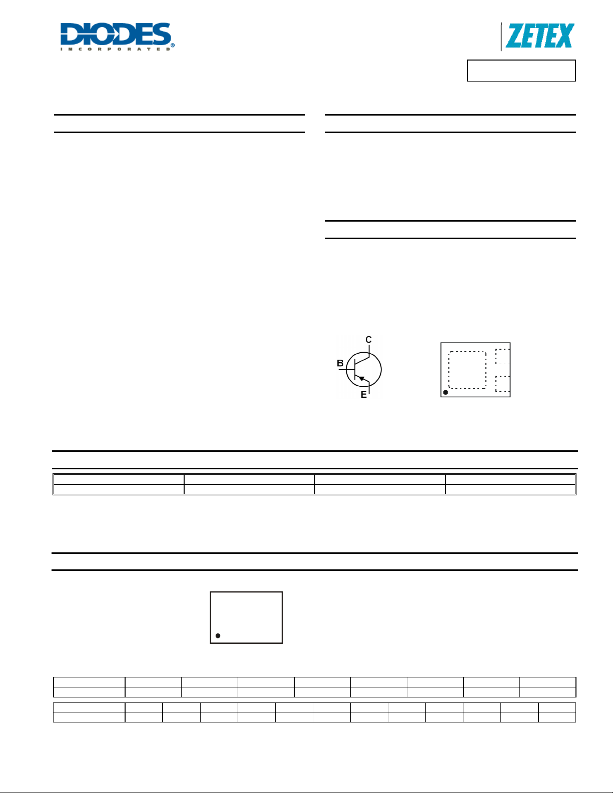
Top view Device Symbol Bottom view
) at High IC
FE
CE(SAT)
CE(SAT)
PNP SURFACE MOUNTED TRANSISTOR
Mechanical Data
• Case: DFN1411-3
• Case Material: Molded Plastic, “Green” Molding Compound.
UL Flammability Classification Rating 94V-0
• Moisture Sensitivity: Level 1 per J-STD-020
• Terminals: Finish – NiPdAu over Copper lead frame. Solderable
per MIL-STD-202, Method 208
• Weight: 0.003 grams (approximate)
Applications
• MOSFET and IGBT gate driving
• DC-DC conversion
• Interface between low voltage IC and Load
• Load disconnect switch
Diodes Incorporated
ZXTP26020DMF
E
C
B
Pin-Out Top view
Ordering Information
Product Reel size (inches) Tape width (mm) Quantity per reel
ZXTP26020DMFTA 7 8 3000
Notes: 1. No purposefully added lead. Halogen and Antimony Free.
2. Diodes Inc’s “Green” Policy can be found on our website at http://www.diodes.com
Marking Information
Date Code Key
Year 2009 2010 2011 2012 2013 2014 2015 2016
Code W X Y Z A B C D
Month Jan Feb Mar Apr May Jun Jul Aug Sep Oct Nov Dec
Code 1 2 3 4 5 6 7 8 9 O N D
ZXTP26020DMF
Document number: DS32101 Rev. 1 - 2
Z2
Z2= Product Type Marking Code
YM = Date Code Marking
YM
Y = Year (ex: W = 2009)
M = Month (ex: 9 = September)
1 of 6
www.diodes.com
May 2010
© Diodes Incorporated

A
f
θ
θ
Product Line o
Diodes Incorporated
ZXTP26020DMF
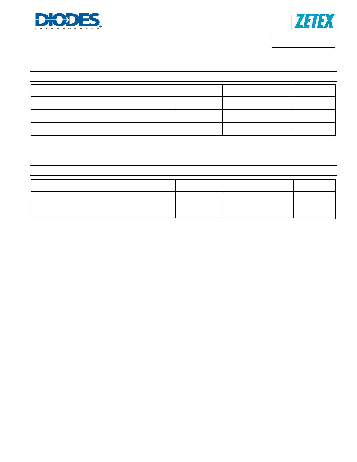
Maximum Ratings
Characteristic Symbol Value Unit
Collector-Base Voltage
Collector-Emitter Voltage
Emitter-Base Voltage
Continuous Collector Current
Peak Pulse Current
Base Current(DC)
Peak Base Current
V
CBO
V
CEO
V
EBO
I
C
I
CM
I
B
I
BM
-20 V
-20 V
-7 V
-1.25 A
-4 A
-0.3 A
-0.6 A
Thermal Characteristics
Characteristic Symbol Value Unit
Power Dissipation (Note 3)
Power Dissipation (Note 4)
Thermal Resistance, Junction to Ambient (Note 3) @ TA = 25°C
Thermal Resistance, Junction to Ambient (Note 4) @ TA = 25°C
Operating and Storage Temperature Range
Notes: 3. Device mounted on FR-4 PCB with 1inch square pads.
4. Device mounted on FR-4 PCB with minimum recommended pad layout
P
P
R
R
T
J, TSTG
D
D
JA
JA
1 W
380 mW
125
330
-55 to +150
°C/W
°C/W
°C
ZXTP26020DMF
Document number: DS32101 Rev. 1 - 2
2 of 6
www.diodes.com
May 2010
© Diodes Incorporated
 Loading...