

Page 1
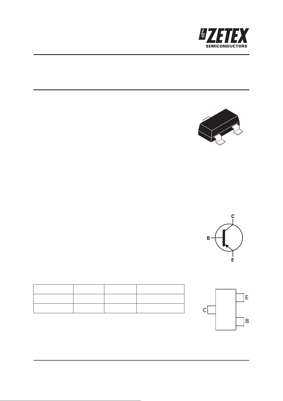
ZXTP2039F
SOT23 80 volt PNP silicon planar medium power
transistor
Summary
V
(BR)CEV
V
(BR)CEO
I
c(cont)
V
ce(sat)
> -80V
> -60V
= -1A
< -600mV @ -1A
Complementary type
ZXTN2038F
Description
This transistor combines high gain, high current operation and low saturation voltage making it
ideal for power MOSFET gate driving and low loss power switching.
Features
■ Low saturation voltage for reduced power dissipation
■ 1 to 2 amp high current capability
■ Pb-free
■ SOT23 package
Applications
■ Power MOSFET gate driving
■ Low loss power switching
Ordering information
Pin out - top view
Device Reel size Tape width Quantity per reel
ZXTP2039FTA 7” 8mm 3,000
ZXTP2039FTC 13” 8mm 10,000
Device marking
P39
Issue 3 - August 2005 1 www.zetex.com
© Zetex Semiconductors plc 2005
Page 2
ZXTP2039F
Absolute maximum ratings
Parameter Symbol Limit Unit
Collector-base voltage V
Collector-emitter voltage V
Collector-emitter voltage V
Emitter-base voltage V
Peak pulse current I
Continuous collector current
*
Peak base current I
Power dissipation @ T
A
=25°C
*
Operating and storage temperature T
NOTES:
* For a device surface mounted on a 15mm x 15mm FR4 PCB with high coverage of single sided 1oz copper, in still air
conditions.
CBO
CEV
CEO
EBO
CM
I
C
BM
P
D
j:Tstg
-80 V
-80 V
-60 V
-5.0 V
-2 A
-1 A
-1 A
350 mW
-55 to +150 °C
Issue 3 - August 2005 2 www.zetex.com
© Zetex Semiconductors plc 2005
Page 3

ZXTP2039F
Electrical characteristics (@T
AMB
= 25°C)
Parameter Symbol Min. Max. Unit Conditions
Collector-base breakdown
V
(BR)CBO
-80 V IC=-100A
voltage
Collector-emitter breakdown
voltage
Collector-emitter breakdown
voltage
Emitter-base breakdown
V
(BR)CEV
V
(BR)CEO
V
(BR)EBO
-80 V IC=-1A
-0.3V < V
-60 V
=-10mA
I
C
-5 V IE=-100µA
voltage
Collector-emitter cut-off current I
Collector-base cut-off current I
Emitter-base cut-off current I
Static forward current transfer
ratio
CES
CBO
EBO
h
FE
100
100
80
15
-100 nA VCE=-60V
-100 nA VCB=-60V
-100 nA VEB=-4V
I
=-1mA, VCE=-5V
C
I
300
=-500mA, VCE=-5V
C
IC=-1A, VCE=-5V
IC=-2A, VCE=-5V
BE
*
< 1V
*
*
*
Collector-emitter saturation
voltage
V
CE(sat)
-0.2
-0.3
-0.6
Base-emitter saturation voltage V
Base-emitter turn-on voltage V
Transition frequency f
Output capacitance C
NOTES:
* Measured under pulsed conditions. Pulse width=300S. Duty cycle ⱕ2%
Spice parameter data is available upon request for this device
BE(sat)
BE(on)
T
obo
150 IC=-50mA, VCE=-10V
-1.2 V
-1.0 V
10 pF VCB=-10V, f=1MHz
V
I
=-100mA, IB=-2mA*
V
V
C
I
=-500mA, IB=-50mA
C
IC=-1A, IB=-100mA
=-1A, IB=-100mA
I
C
=-1A, VCE=-5V
I
C
f=100MHz
*
*
*
*
Issue 3 - August 2005 3 www.zetex.com
© Zetex Semiconductors plc 2005
Page 4

Typical characteristics
ZXTP2039F
-(V)
CE(sat)
V
- Typical Gain
FE
h
0.6
0.5
0.4
0.3
0.2
0.1
0
400
300
200
100
1mA
V
+25 ° C
CE
=5V
+100 °C
+25 °C
-55 °C
IC/IB=10
IC/IB=50
100mA10mA
IC-Collector Current
CE(sat)
V
v I
C
0.6
C/IB
=10
I
0.5
0.4
-(V)
0.3
CE(sat)
0.2
V
0.1
10A1A
0
1mA
-55 °C
+25 °C
+100 °C
10A1A10mA 100mA
IC-Collector Current
CE(sat)
- (V)
BE(sat)
V
1.0
0.8
0.6
0.4
0.2
V
C/IB
=10
I
v I
C
+100 °C
-55 °C
+25 °C
- (V)
BE(on)
V
1.2
1.0
0.8
0.6
0.4
0.2
0
0
1mA
1mA
0
100mA10mA
-Collector Current
I
C
hFEV I
CE
V
=5V
100mA10mA
1A
10A
C
-55 °C
+25 °C
+100 °C
1A
10A
1mA
10
1
0.1
-Collector Current (A)
C
I
0.01
0.1V 10V 100V
IC-Collector Current
BE(on)
V
v I
C
10mA
I
C
DC
1s
100ms
10ms
1ms
100us
VCE- Collector Emitter Voltage (V)
Safe Operating Area
100mA 1A 10A
-Collector Current
BE(sat)
V
1V
v I
C
Issue 3 - August 2005 4 www.zetex.com
© Zetex Semiconductors plc 2005
Page 5

Packaging details - SOT23
L
ZXTP2039F
H
N
D
G
3 leads
M
B
A
C
K
F
Package dimensions
Dimensions in inches are control dimensions, dimensions in millimeters are approximate.
Dim. Millimeters Inches Dim. Millimeters Inches
Min. Max. Min. Max. Min. Max. Max. Max.
A 2.67 3.05 0.105 0.120 H 0.33 0.51 0.013 0.020
B 1.20 1.40 0.047 0.055 K 0.01 0.10 0.0004 0.004
C - 1.10 - 0.043 L 2.10 2.50 0.083 0.0985
D 0.37 0.53 0.015 0.021 M 0.45 0.64 0.018 0.025
F 0.085 0.15 0.0034 0.0059 N 0.95 Nom. 0.0375 Nom.
G 1.90 Nom. 0.075 Nom. - - - - -
Europe
Zetex GmbH
Streitfeldstraße 19
D-81673 München
Germany
Telefon: (49) 89 45 49 49 0
Fax: (49) 89 45 49 49 49
europe.sales@zetex.com
These offices are supported by agents and distributors in major countries world-wide.
This publication is issued to provide outline information only which (unless agreed by the company in writing) may not be used, applied or
reproduced for any purpose or form part of any order or contact or be regarded as a representation relating to the products or services concerned.
The company reserves the right to alter without notice the specification, design, price or conditions of supply of any product or service.
Americas
Zetex Inc
700 Veterans Memorial Highway
Hauppauge, NY 11788
USA
Telephone: (1) 631 360 2222
Fax: (1) 631 360 8222
usa.sales@zetex.com
Asia Pacific
Zetex (Asia Ltd)
3701-04 Metroplaza Tower 1
Hing Fong Road, Kwai Fong
Hong Kong
Telephone: (852) 26100 611
Fax: (852) 24250 494
asia.sales@zetex.com
Corporate Headquarters
Zetex Semiconductors plc
Zetex Technology Park, Chadderton
Oldham, OL9 9LL
United Kingdom
Telephone (44) 161 622 4444
Fax: (44) 161 622 4446
hq@zetex.com
Issue 3 - August 2005 5 www.zetex.com
© Zetex Semiconductors plc 2005
 Loading...