Diodes ZXSC400 User Manual
LED DRIVER BOOST CONVERTER
DESCRIPTION
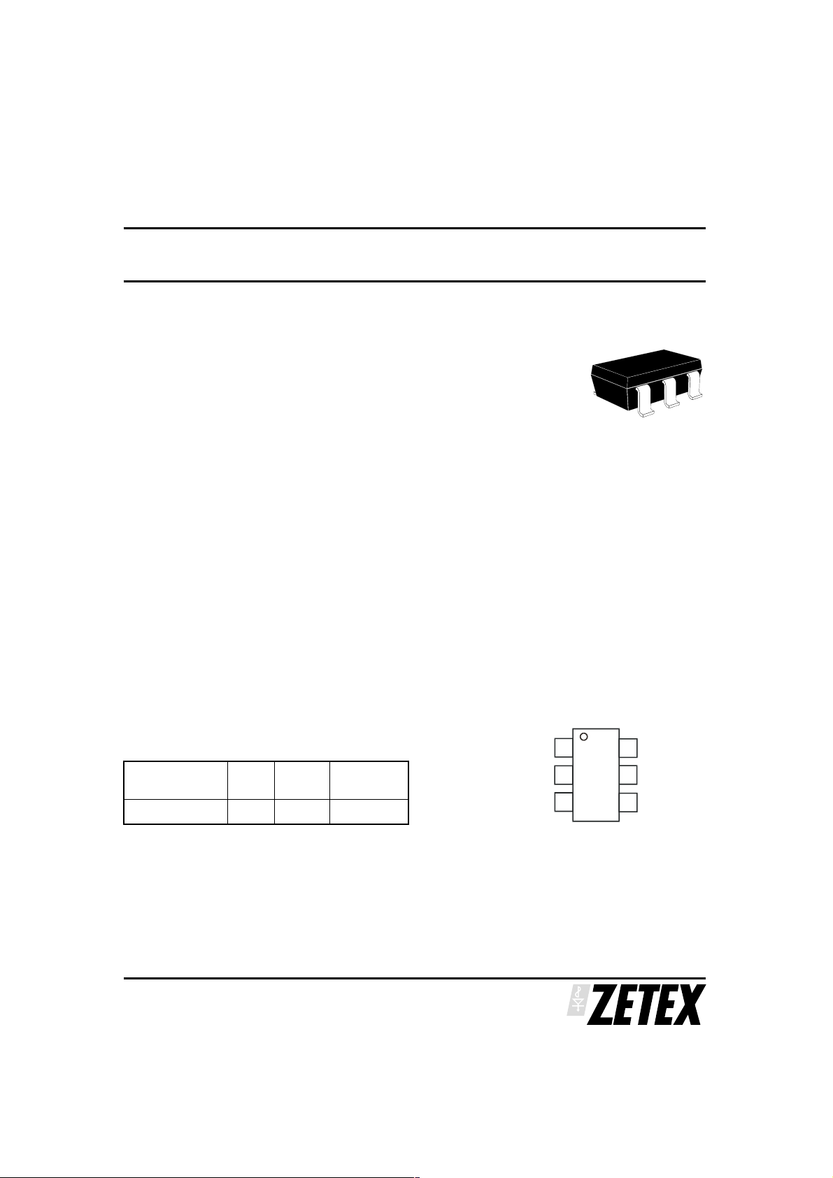
The ZXSC400 is a voltage mode boost converter in the SOT23-6 package. Its low
feedback voltage allows the current in a chain of LEDs to be set and accurately
monitored with asingle resistor giving minimal losses. Its excellent load and line
regulation means that for the full supply range from lithium-ion cells, the LED
currentwilltypicallychangebyless than 1%.Usinghigh efficiency Zetexswitching
transistorswith ratings of 20V and higher allowmany LEDs to be chained inseries
for the best LED current matching possible.
ZXSC400
FEATURES
1.8V to 8V supply range
•
Typical output regulation of ⫾1%
•
Over 80% typical efficiency
•
4.5A typical shutdown current
•
Series connection for ultimate LED current matching
•
APPLICATIONS
•
White LED backlighting for colour LCD panels
•
General LED backlighting
•
High performance white LED flashlights
•
General LED driving from batteries
ORDERING INFORMATION
DEVICE REEL
ZXSC400E6TA
SIZE
7“ 8mm 3000 units
TAPE
WIDTH
QUANTITY
PER REEL
DEVICE MARKING
•
C400
PINOUT
V
CC
GND
STDN
Top View
T
O
S
-
6
3
2
DRIVE
V
FB
SENSE
ISSUE 1 - JANUARY 2003
1
ZXSC400
ABSOLUTE MAXIMUM RATINGS
V
CC
DRIVE -0.3V to V
EOR -0.3V to V
STDN -0.3V to The lower of (+5.0V) or (V
SENSE -0.3V to The lower of (+5.0V) or (V
Operating Temp. -40°C to +85°C
Storage Temp. -55°C to +125°C
Power Dissipation 450mW
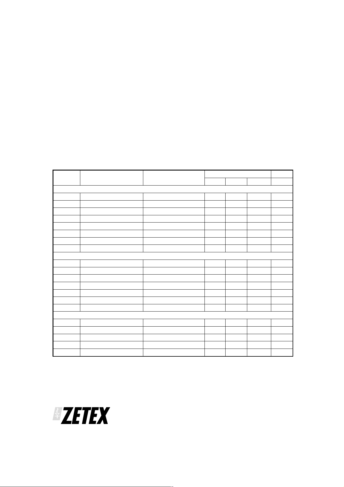
ELECTRICAL CHARACTERISTICS
Test Conditions V
Symbol Parameter Conditions Limits Units
Supply parameters
V
IN
1
Iq
I
STDN
1
Eff
Acc
REF
TCO
REF
T
DRIVE
F
OSC
Input parameters
V
SENSE
I
SENSE
V
FB
2
I
FB
V
IH
V
IL
dV
LN
Output parameters
3
I
OUT
I
DRIVE
V
DRIVE
C
DRIVE
4
dILD
Note
1
Excluding gate/base drive current.
2
IFBis typically half these values at 300mV.
3
System not device spec, including recommended transistors. 10.5V represents 3 white LEDs.
4
Change in LED current with changing supply voltage (LED VFx number of series LEDs).
-0.3V to +10V
+ 0.3V
CC
+ 0.3V
CC
= 3V, T= -40°C to 85°C unless otherwise stated.
CC
CC
CC
+ 0.3V)
+ 0.3V)
Min Typ Max
VCCRange 1.8 8 V
Quiescent Current VCC= 8V 220 A
Shutdown Current 4.5 A
Efficiency 30mA > I
> 10mA 80 %
LED
Reference tolerance 1.8V < VCC< 8V -3.0 3.0 %
Reference Temp Co 0.005 %/⬚C
Discharge pulse width 1.8V < VCC<8V 1.7 s
Operating Frequency 200 kHz
Sense voltage 22 28 34 mV
Sense input current VFB=0V,V
= 0V -1 -7 -15 A
SENSE
Feedback voltage 291 300 309 mV
Feedback input current VFB=0V,V
Shutdown high voltage 1.5 V
= 0V -1.2 -4.5 A
SENSE
CC
Shutdown low voltage 0 0.55 V
Line voltage regulation 0.5 %/V
Output current Vin > 2V, Vout = 10.5V 50 mA
Transistor drive current Vdrive = 0.7V 2 3.5 5 mA
Transistor voltage drive 1.8V < VCC<8V 0 V
-0.4 V
CC
Mosfet gate drive cpbty 300 pF
Load current regulation 0.1 mA/V
V
ISSUE 1 - JANUARY 2003
2
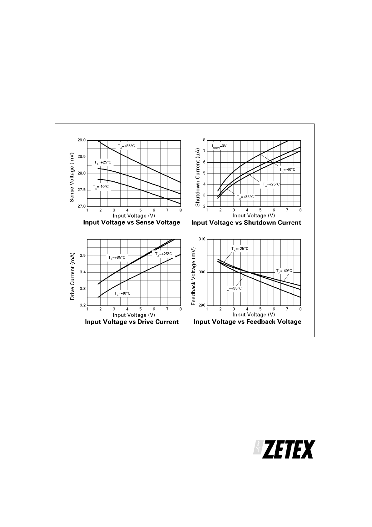
TYPICAL CHARACTERISTICS
ZXSC400
ISSUE 1 - JANUARY 2003
3
ZXSC400
DESIGN INFORMATION
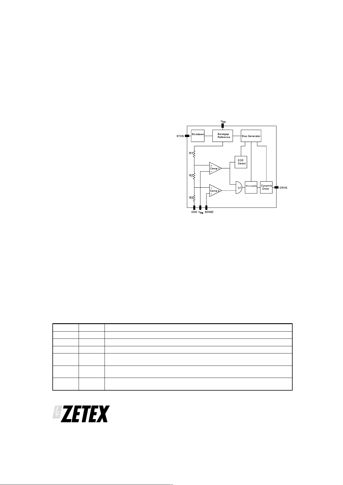
IC operation description
Bandgap Reference
All threshold voltages and internal currents are
derived from a temperature compensated bandgap
reference circuit with a reference voltage of 1.22V
nominal.
Dynamic Drive Output
Depending on the input signal, the output is either
“LOW” or “HIGH”. In the high state a 2.5mA current
source (max drive voltage = V
or gate of the external transistor. In order to operate
the external switching transistor at optimum
efficiency, both output states are initiated with a short
transientcurrent in order to quickly discharge the base
or the gate of the switching transistor.
Switching Circuit
The switching circuit consists of two comparators,
Comp1 and Comp2, a gate U1, a monostable and the
driveoutput.Normally the DRIVE output is “HIGH”; the
external switching transistor is turned on. Current
ramps up in the inductor, the switching transistor and
external current sensing resistor. This voltage is
sensed by comparator, Comp2, at input I
the current sense voltage across the sensing resistor
exceeds 30mV, comparator Comp2 through gate U1
triggers a re-triggerable monostable and turns off the
output drive stage for 2s. The inductor discharges to
the load of the application. After 2s a new charge
cycle begins, thus ramping the output voltage. When
the output voltage reaches the nominal value and FB
gets an input voltage of more than 300mV, the
monostable is forced “on” from Comp1 through gate
U1, until the feedback voltage falls below 300mV. The
above action continues to maintain regulation.
-0.4V) drives the base
CC
. Once
SENSE
Block diagram
2µs
Pin functions
Pin No. Name Description
1V
2 GND Ground
3 STDN Shutdown
4 SENSE
5
6 DRIVE
CC
V
FB
Supply voltage, 1.8V to 8V.
Inductor current sense input. Internal threshold voltage set to 30mV. Connect
external sense resistor
Reference voltage. Internal threshold set to 300mV. Connect external resistor
to program LED current
Drive output for external switching transistor. Connect to base or gate of
external switching transistor.
ISSUE 1 - JANUARY 2003
4
APPLICATIONS INFORMATION
ZXSC400
Switching transistor selection
The choice of switching transistor has a major impact
ontheconverterefficiency.Foroptimumperformance,
a bipolar transistor with low V
required.TheV
important parameter as this sees the full output
oftheswitchingtransistorisalsoan
CEO
and high gain is
CE(SAT)
voltage when the transistor is switched off. Zetex
SuperSOT™ transistors are an ideal choice for this
application.
Schottky diode selection
As with the switching transistor, the Schottky rectifier
diodehasamajor impact on the converter efficiency. A
Schottky diode with a low forward voltage and fast
recovery time should be used for this application.
The diode should be selected so that the maximum
forward current rating is greater or equal to the
maximum peak current in the inductor, and the
maximum reverse voltage is greater or equal to the
output voltage. The Zetex ZHCS Series meet these
needs.
Combination devices
To minimise the external component count Zetex
recommends the ZX3CDBS1M832 combination of
NPN transistor and Schottky diode in a 3mm x 2mm
MLP package. This device is recommended for use in
applications using 1 to 4 white LEDs.
Capacitor Selection
Asmall value, low ESR ceramic capacitor isrequired to
filter the output, typically 1F to 4.7F.
Generallyan input capacitor is notrequired,buta small
ceramic capacitor may be added to aid EMC, typically
1F to 4.7F.
Inductor Selection
The inductor value must be chosen to satisfy
performance, cost and size requirements of the overall
solution.
Inductor selection has a significant impact on the
converter performance. For applications where
efficiencyis critical, an inductor withaseriesresistance
of 250m⍀ or less should be used.
A list of recommended inductors is listed in the table
below:
The IC is also capable of driving MOSFETs. Zetex
recommends the ZXMNS3BM832 combination of low
threshold voltage N-Channel MOSFET and Schottky
diode in a 3mm x 2mm MLP package. This device is
recommendedfor use in applications using1to8 white
LEDs.
Part No. Manufacture L I
CMD4D11-100MC Sumida 10H 0.5 0.457
CMD4D11-220MC Sumida 22H 0.4 0.676
LPO2506OB-103 Coilcraft 10H 1.0 0.24
ST2006103 Standex Electronics Inc 10H 0.6 0.1
(A) RDC( )
PK
ISSUE 1 - JANUARY 2003
5
 Loading...