

Page 1
SEMICONDUCTORS
LED DRIVER SOLUTION FOR LCD BACKLIGHTING
V
IN
V
CC
V
=3.3V/5V
DRIVE
I
SENSE
Gnd
S
TDN
DEVICE DESCRIPTION
ZXSC310
The ZXSC310 is a single or multi cell LED driver
designed for LCD backlighting applications. The input
voltage range of the device is between 0.8V and 8V.
This means the ZXSC310 is compatible with single
NiMH, NiCd or Alkaline cells, as well as multi-cell or
LiIon batteries.
The device features a shutdown control, resulting in a
standby current less than 5µA, and an output capable
of driving serial or parallel LED’s. The circuit generates
constant power output, which are ideal for driving
single or multiple LED’s over a wide range of operating
voltages. These features make the device ideal for
driving LED’s particularly in LCD backlight applications
for Digital Still cameras and PDA’s.
FEATURES
• 94% efficiency
• Minimum operating input voltage 0.8V
• Maximum operating input voltage 8V
• Standby current less than 5µA
• Programmable output current
• Series or parallel LED configuration
• Low saturation voltage switching transistor
•
SOT23-5 package
APPLICATIONS
•
LCD backlights:
Digital still camera
PDA
Mobile phone
•
LED flashlights and torches
•
White LED driving
•
Multiple LED driving
ORDERING INFORMATION
The ZXSC310 is a PFM DC-DC controller IC that drives
an external Zetex switching transistor with a very low
saturation resistance. These transistors are the best
switching devices available for this type of conversion
enabling high efficiency conversion with low input
voltages. The drive output of the ZXSC310 LED driver
generates a dynamic drive signal for the switching
transistor.
The circuit can start up under full load and operates
down to an input voltage of 0.8 volts. The solution
configuration ensures optimum efficiency over a wider
range of load currents; several circuit configurations
are possible depending on battery life versus
brightness considerations.
The ZXSC310 is offered in the SOT23-5 package which,
when combined with a SOT23 switching transistor,
generates a high efficiency small size circuit solution.
The IC and discrete combination offers the ultimate
cost Vs performance solution for LED backlight
applications.
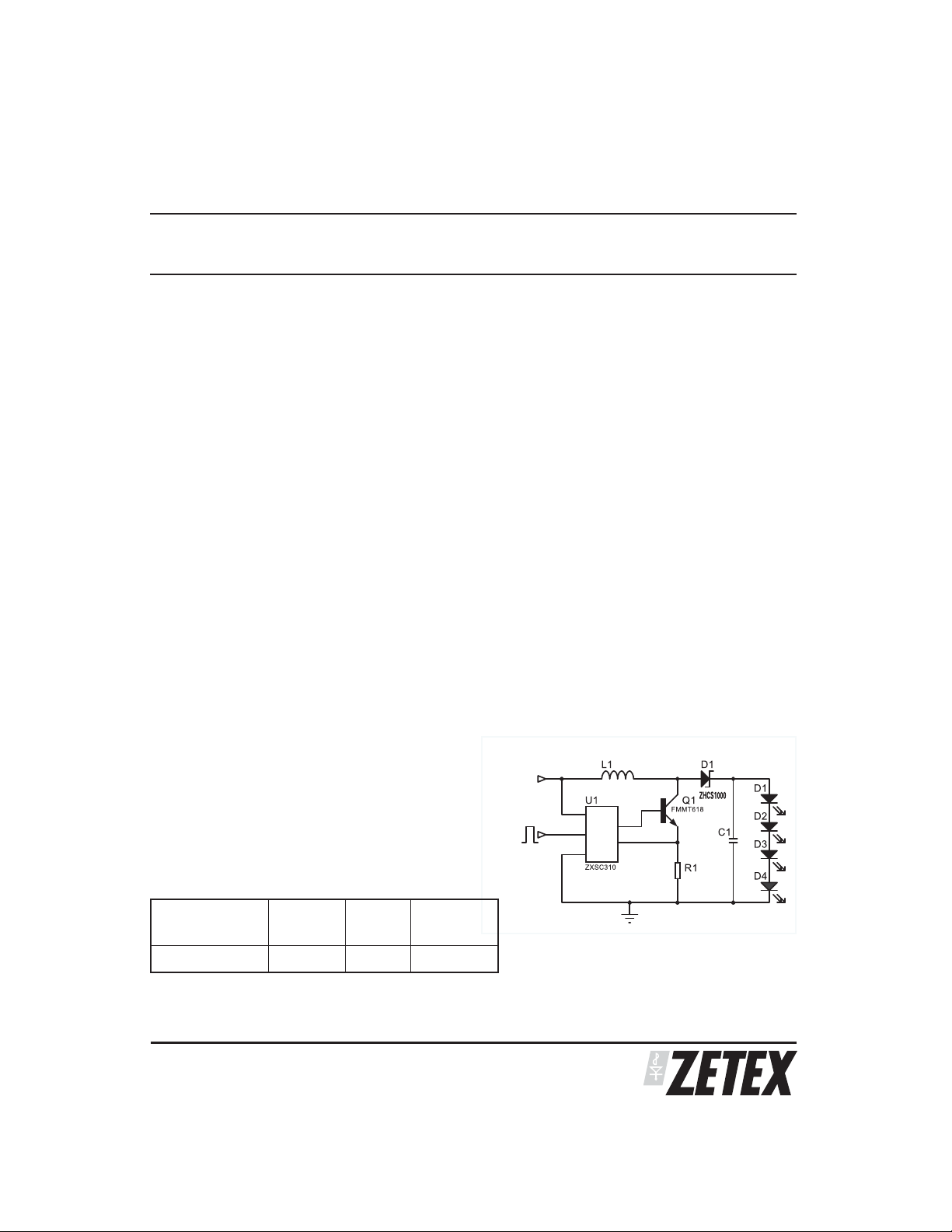
TYPICAL APPLICATIONS CIRCUIT
DEVICE REEL
SIZE
ZXSC310E5TA 180mm 8mm 3000
TAPE
WIDTH
QUANTITY
PER REEL
DEVICE MARKINGS
•
C310
Package SOT23-5
ISSUE 3 - SEPTEMBER 2007
1
Page 2
SEMICONDUCTORS
ZXSC310
ABSOLUTE MAXIMUM RATINGS:
Supply Voltage -0.3 to 10V
Maximum Voltage other pins -0.3 to V
Power Dissipation 450mW
Operating Temperature -40 to 85 °C
Storage Temperature -55 to 150°C
ELECTRICAL CHARACTERISTICS:
Test conditions unless otherwise stated: V
Symbol Parameter Conditions Min Typ Max Units
Efficiency
V
CC
V
CC(min)
I
Q
I
VDRIVE
I
CC
Recommended supply
voltage range
Minimum startup and
operating voltage
Quiescent current
Base drive current V
Supply current
(1)
(2)
(3)
CC
I
=-600µA,V
DRIVE
=-600µA, V
I
DRIVE
T
=-10°C
AMB
V
EN =VCC
0V (standby)
V
EN =
DRIVE
V
DRIVE
=1.5V, T
(3)
(enabled)
=0.7V,V
=0.7V,V
+0.3V
CC
=25 C
AMB
0.8 8 V
DRIVE
DRIVE
=0.7V
=0.7V,
0.8
0.9
0.2
510mAµA
=0V 1.5 3.5 mA
ISENSE
=0V 2 4 mA
ISENSE
94 %
0.92 V
V
VDRIVE(high)
V
VDRIVE(low)
V
STDN(high)
V
STDN(low)
I
STDN
V
ISENSE
(threshold)
T
CVISENSE
I
ISENSE
T
DRV
High level drive voltage V
Low level drive voltage V
ISENSE
ISENSE
=0V,I
VDRIVE
= 50mV, I
=-0.5mA V
=5mA 0 0.2 V
VDRIVE
Device enabled 0.7 V
Device in standby mode 0.15 V
Enable input current -1 1 µA
Output current reference
voltage
I
voltage temp co.
SENSE
I
input current V
SENSE
(2)
=0V 0 -30 -65 µA
ISENSE
Discharge Pulse Width 1.2 1.7 3.2 µs
OPERATING CONDITIONS
Symbol
F
OSC
(1) Application dependent, see reference designs
(2) These parameters guaranteed by Design and characteristics
(3) Total supply current =I
(4) Operating frequency is application circuit dependent. See applications section.
Parameter Conditions Min Typ Max Units
Recommended operating
frequency
Q+IVDRIVE
(4)
, see typical characteristics
CC
V
CC
-0.3
14 19 24 mV
0.4 %/°C
200 kHz
ISSUE 3 - SEPTEMBER 2007
V
2
Page 3
ZXSC310
SEMICONDUCTORS
FMMT618
For the circuits described in the applications section
Zetex FMMT618 is the recommended pass transistor.
ELECTRICAL CHARACTERISTICS:
Test conditions unless otherwise stated: T
Symbol Parameter Conditions Min Typ Max Units
V
CE(sat)
V
(BR)CEO
5
Measured under pulse conditions. Pulse width=300µs. Duty cycle ⱕ2%
Collector-Emitter
Saturation Voltage
Collector-Emitter
Breakdown Voltage
5
5
IC=0.1A, IB=10mA
I
C
I
C
IC=10mA 20 27 V
ZHCS1000
The following indicates outline data for the device,
more detailed information can be found at
www.zetex.com/fmmt618
=25 C
AMB
8
=1A, IB=10mA
=2.5A, IB=50mA
70
130
15
150
200
mV
For the maximum brightness circuit described in the
applications section Zetex ZHCS1000 is the
recommended Schottky diode.
The following indicates outline data for the ZHCS, more
detailed information can be found at
www.zetex.com/zhcs1000
ELECTRICAL CHARACTERISTICS:
Test conditions unless otherwise stated: T
Symbol Parameter Conditions Min Typ Max Units
V
F
t
rr
I
R
Part
Number
BAT54 30 200 0.6 500 30 250 25 10 SOT23-6
ZHCS2000 40 2000 20 500 2000 1000 30 60 SOT23
ZHCS1000 40 1000 12 500 1000 100 30 25 SOT23
ZHCS750 40 750 12 540 750 100 30 25 SOT23
ZHCS500 40 500 6.75 550 500 40 30 20 SOT23
ZHCS400 40 400 6.75 500 400 40 30 20 SOT323
Forward voltage IF= 500mA
I
F
Reverse Recovery Time Switched from IF=500mA to
I
R
Measured at I
Reverse Current VR= 30V 50 100 µA
V
Max.VMax.mAMax.AMax.mVI
I
R
I
F
FSM
VFat IRat Capacitance
F
mA
AMB
=1A
=500mA.
Max.AV
=25 C
=50mA
R
R
V
=25V,f=1MHz
at V
R
Typ.
400
500
12 ns
Package
SOT23
pF
mV
ISSUE 3 - SEPTEMBER 2007
3
Page 4
SEMICONDUCTORS
ZXSC310
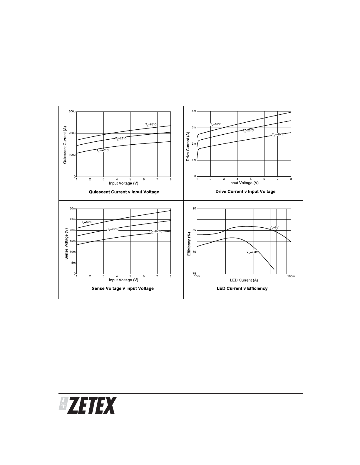
TYPICAL CHARACTERISTICS
ISSUE 3 - SEPTEMBER 2007
4
Page 5
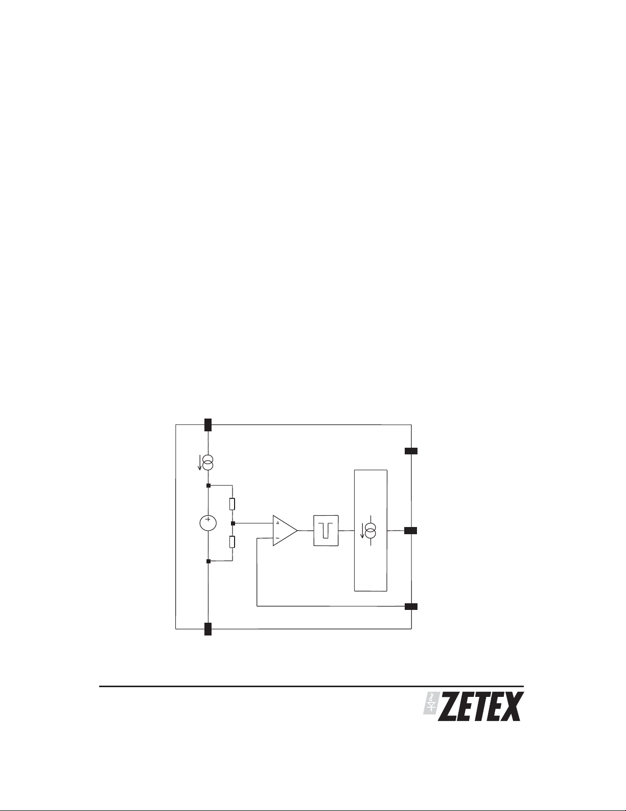
DEVICE DESCRIPTION
SEMICONDUCTORS
I
2
Drive
I
SENSE
R2
V
RE
R1
V
DRIVE
G
N
D
I
V
CC
S
TDN
ZXSC310
The ZXSC310 is PFM, controller IC which, when
combined with a high performance external transistor,
enables the production of a high efficiency boost
converter for LED driving applications. A block diagram
is shown for the ZXSC310 below.
The on chip comparator forces the driver circuit and
therefore the external switching transistor off if the
voltage at I
circuit and divider set this threshold.
The voltage at I
resistor connected in series with the emitter of the
switching transistor. A monostable following the
output of the comparator forces the turn-off time of the
output stage to be typically 1.7us. This ensures that
there is sufficient time to discharge the inductor coil
before the next on period.
exceeds 19mV. An internal reference
SENSE
is taken from a current sense
SENSE
With every on pulse the switching transistor is kept on
until the voltage across the current-sense resistor
exceeds the threshold of the I
length, and therefore the switching frequency, is
determined by the programmed peakcurrent,theinput
voltage and the inputto output voltage differential. See
applications section for details.
The driver circuit supplies the external switching
transistor with a fixed drive current. To maximise
efficiency the external transistor switched quickly,
typically being forced off within 30ns.
input. The on-pulse
SENSE
ZXSC310 Block Diagram
ISSUE 3 - SEPTEMBER 2007
5
Page 6

SEMICONDUCTORS
ZXSC310
V
IN
V
CC
V
=3.3V/5V
DRIVE
I
SENSE
Gnd
S
TDN
REFERENCE DESIGNS
Three typical LED driving applications are shown.
Firstly a typical LCD backlight circuit, then maximum
brightness LED driving solution and lastly an optimised
battery life LED driving solution.
LCD backlight circuit
This application shows the ZXSC310 in a typical LCD
backlight application for Digital Still Cameras and
PDA’s. The input voltage for these backlightcircuits are
usually fixed from the main system power, typically
3.3V or 5V. The LED’s are connected serially so that the
light is distributed uniformly in each LED. The current
provided to the LED’s can either be pulsed or DC. The
DC current is programmable via a sense resistor,
R
, and is set to an optimum LED current of 20mA
SENSE
for the reference designs. DC current is achieved by
adding a Schottky rectifying diode and an output
capacitor, as shown in the reference design below.
(Notes)
Materials list
Ref Value Part Number Manufacture Comments
U1 N/A ZXSC310E5 Zetex Semiconductors Sing le cell c onv erter, S OT2 3-5
Q1 N/A FM MT6 18 Zetex Semiconductors Lo w V
D1 N/A ZHCS10 00 Zetex Semiconductors 1A S cho ttky diode , S OT2 3
C1 2.2F Generic Various 0805 Size
(6)
R1
R1
L1
(6)
Used for 3.3V input, I
(7)
Used for 5V input, I
(8)
See Application section.
150m⍀ Generic Various 1206 Size
(8)
(7)
250m⍀
68µH Surface mount inductor
Generic Various 1206 Size
set to 20mA ⫾10%.
LED
to 20mA ⫾10%.
LED
6
NPN, SOT23
CE(sat)
ISSUE 3 - SEPTEMBER 2007
Page 7

ZXSC310
SEMICONDUCTORS
Q1
FMMT617
R1
L1
V
D2
CC
G
I
V
S
U1
ZXSC310
D1
ZHCS1000
C1
BATT
V
DRIVE
TDN
SENSE
ND
Maximum brightness solution
This circuit provides a continuous current output to the
LED by rectifying and buffering the DC-DC output. This
ensures maximum LED brightness.
(Notes)
Materials list
Ref Value Part Number Manufacturer Comments
U1 N/A ZXSC310E5 Zetex Plc Single cell converter, SOT23-5
Q1 N/A FMMT617 Zetex Plc Low
D1 1A ZHCS1000 Zetex Plc 1A Shottky diode, SOT23
R1 100m⍀ Generic Various 0805 Size
C1 2.2F
L1 100µH
(8)
See Application section.
(8)
Generic Various Low ESR ceramic capacitor
Surface mount inductor
ISSUE 3 - SEPTEMBER 2007
7
VCE(sat)
NPN, SOT23
Page 8

SEMICONDUCTORS
ZXSC310
Maximum battery life solution
To ensure optimum efficiency, and therefore
maximum battery life, the LED is supplied with a pulsed
current. Maximum efficiency is ensured with the
removal of rectifier losses experienced in the
maximum brightness solution.
(Notes)
Materials list
Ref Value Part Number Manufacturer Comments
U1 N/A ZXSC310E5 Zetex Semiconductors Si ng le c ell co nvert er , SO T23-5
Q1 N/A FMMT6 17 Zetex Semiconductors Lo w V
R1 330m⍀ Generic Various 0805 Size
L1 100H
(8)
See Application section.
(8)
8
Surface mount inductor
NPN, SOT23
CE(sat)
ISSUE 3 - SEPTEMBER 2007
Page 9

APPLICATIONS INFORMATION
SEMICONDUCTORS
0.
0
0.4
0.
1
0.2
0.
3
ZXSC310
The following section is a design guide for optimum
converter performance.
Switching transistor selection
The choice of switching transistor has a major impact
on the converter efficiency. For optimumperformance,
a bipolar transistor with low V
required.
The Zetex FMMT618 is an ideal choice of transistor,
having a low saturation voltage. A data sheet for the
FMMT618 is available on Zetex web site or through
your local Zetex sales office. Outline information is
included in the characteristics section of this data
sheet.
and high gain is
CE(SAT)
Schottky diode selection
For the maximum battery life solution a Schottky
rectifier diode is not required. As with the switching
transistor the Schottky rectifier diode has a major
impact on the converter efficiency. A Schottky diode
with a low forward voltage and fast recovery time
should be used for this application.
The diode should be selected so that the maximum
forward current is greater or equal to the maximum
peak current in the inductor, and the maximum reverse
voltage is greater or equal to the output voltage.
The Zetex ZHCS1000 meets these needs. Datasheets
for the ZHCS Series are available on Zetex web site or
through your local Zetex sales office. Outline
information is included in the characteristics section of
this data sheet.
For the maximum brightness solution a pulsed current
is supplied to the LED and thus a Schottky rectifier
diode is required.
Inductor selection
The inductor value must be chosen to satisfy
performance, cost and size requirements of the overall
solution. For the LCD backlight reference design we
recommend an inductor value of 68uH with a core
saturation current rating greater than the converter
peak current value and low series resistance.
Inductor selection has a significant impact on the
converter performance. For applications where
efficiency is critical, aninductorwith a series resistance
of 500m⍀ or less should be used.
A list of recommended inductors is shown in the table
below:
Part No. Manufacture L I
DO1608C-683 Coilcraft 68H 0.4A 0.86⍀
CR54-680 Sumida 68H 0.61A 0.46⍀
P1174.683 Pulse 68H 0.4A 0.37⍀
SFOP5845-R61680 Samwha 68H 0.61A 0.46⍀
SIS43-680 Delta 68H 0.4 1.125⍀
PK
R
DC
ISSUE 3 - SEPTEMBER 2007
9
Page 10

SEMICONDUCTORS
ZXSC310
Peak current definition
The peak current rating is a design parameter whose
value is dependent upon the overall application. For
the high brightness reference designs, a peak current
of 190mA was chosen to ensure that the converter
could provide the required output power to the LED.
In general, the I
value must be chosen to ensure that
PK
the switching transistor, Q1, is in full saturation with
maximum output power conditions, assuming
worse-case input voltage and transistor gain under all
operating temperature extremes.
Input Voltage
(V)
3.3V 10 3 510 68 80
3.3V 10 4 330 68 81
3.3V 10 6 150 68 79
3.3V 20 3 220 68 84
3.3V 20 4 150 68 93
3.3V 20 6 77 68 79
3.3V 30 3 170 68 84
3.3V 30 4 100 68 84
3.3V 30 6 47 68 77
5V 10 3 750 68 83
5V 10 4 510 68 84
5V 10 6 330 68 79
5V 20 3 440 68 85
5V 20 4 250 68 85
5V 20 6 150 68 82
5V 30 3 330 68 86
5V 30 4 170 68 85
5V 30 6 100 68 83
LED current
(mA)
No. of LED’s R
Once I
is decided the value of R
PK
SENSE
can be
determined by:
ISENSE
SENSE
=
Inductor
( H)
V
PK
I
Efficiency
(%)
R
A selection guide of sense resistor and inductor values
for given input voltages, output currents and number
of LED connected in series is provided in the table
below.
SENSE
(m )
ISSUE 3 - SEPTEMBER 2007
10
Page 11

ZXSC310
SEMICONDUCTORS
Output Power Calculation
By making the above assumptions for inductance and
peak current the output power can be determined by:
OFF
PVVI
OUT OUT IN AV
=−××
()
Note:V
drop.
=output voltage + Schottky rectifier voltage
OUT
Where
1.7us (internally set by ZXSC310)
T
≅
OFF
and
TV V
T
ON
=
−
OFF OUT IN
()
V
IN
and
PK MIN
II
+
I
AV
=
2
T
ON OFF
TT
+
Capacitor selection
For pulsed operation, as in the maximum battery life
solution, no capacitors are required at the output to the
LED. For rectified operation, as in the maximum
brightness solution, a small value ceramic capacitor is
required, typically 2.2uF.
Generally an input capacitorisnot required, but a small
ceramic capacitor may be added to aid EMC, typically
470nF to 1uF.
(notes)
Where
VVT
−×
OUT IN OFF
II
MIN PK
()
=−
L
Operating frequency can be derived by:
F
1
=
ON OFF
TT
+
()
ISSUE 3 - SEPTEMBER 2007
11
Page 12

SEMICONDUCTORS
ZXSC310
Shutdown Control
The ZXSC310 offers a shutdown mode that produces a
standby current of less than 5uA when in operation.
When the voltage at the S
ZXSC310 is enabled, hence the driver is in normal
operation. When the voltage at the S
lower the ZXSC310 is disabled, hence the driver is in
shutdown mode. If the S
ZXSC310 is also enabled.
pin is 0.7V or higher the
TDN
pin is 0.1V or
TDN
pin is open circuit the
TDN
Demonstration board
A demonstration board for the LCD backlighting
solution, is available upon request. These can be
obtained through your local Zetex office or through
Zetex web pages. For all reference designs Gerber files
and bill of materials can be supplied.
Layout of LCD backlighting solution
Top Silk Drill File
Top Copper Bottom Copper
ISSUE 3 - SEPTEMBER 2007
12
Page 13

SEMICONDUCTORS
STDN
VCC
Gnd
ISENSE
VDRIVE
1
2
3
4
5
Top View
PINOUT DIAGRAM
ZXSC310
PIN DESCRIPTIONS
Pin No. Name Description
1V
2G
3S
4I
5V
ISSUE 3 - SEPTEMBER 2007
CC
nd
TDN
SENSE
DRIVE
Supply voltage, generally Alkaline, NiMH or NiCd single cell
Ground
Shutdown
Inductor current sense input. Internal threshold voltage set to 19mV.
Connect external sense resistor
Drive output for external switching transistor. Connect to base of
external switching transistor.
13
Page 14

SEMICONDUCTORS
ZXSC310
(NOTES)
ISSUE 3 - SEPTEMBER 2007
14
Page 15

ZXSC310
SEMICONDUCTORS
Definitions
Product change
Zetex Semiconductors reserves the right to alter, without notice, specifications, design, price or conditions of supply of any product or service.
Customers are solely responsible for obtaining the latest relevant information before placing orders.
Applications disclaimer
The circuitsin this design/applicationnote are offeredas design ideas. Itis the responsibilityof the userto ensure thatthe circuit isfitfor the user's
application andmeets with theuser's requirements. Norepresentation or warranty isgiven and noliability whatsoever is assumedby Zetex with
respect to the accuracy or use of such information, or infringement of patents or other intellectual property rights arising from such use or
otherwise. Zetex does not assume any legal responsibility or will not be held legally liable (whether in contract, tort (including negligence),
breach ofstatutory duty, restriction orotherwise) for any damages,loss of profit,business,contract, opportunity orconsequential loss in theuse
of these circuit applications, under any circumstances.
Life support
Zetex products are specifically not authorized for use as critical components in life support devices or systems without the express written
approval of the Chief Executive Officer of Zetex Semiconductors plc. As used herein:
A. Life support devices or systems are devices or systems which:
1. are intended to implant into the body
or
2. support or sustain life and whose failure to perform when properly used in accordance with instructions
for use provided in the labeling can be reasonably expected to result in significant injury to the user.
B. A critical component is any component in a life support device or system whose failure to perform can be reasonably expected to cause the
failure of the life support device or to affect its safety or effectiveness.
Reproduction
The product specifications contained in this publication are issued to provide outline information only which (unless agreed by the company in
writing) maynot be used, applied orreproduced for any purposeorform part ofany order or contract orbe regarded as a representationrelating
to the products or services concerned.
Terms and Conditions
All productsare sold subjects toZetex'terms and conditions ofsale, and this disclaimer (savein the event of aconflict between the twowhen the
terms of the contract shall prevail) according to region, supplied at the time of order acknowledgement.
For the latest information on technology, delivery terms and conditions and prices, please contact your nearest Zetex sales office.
Quality of product
Zetex is an ISO 9001 and TS16949 certified semiconductor manufacturer.
To ensure quality of service and productswe strongly advise the purchase of parts directly from Zetex Semiconductors or one of our regionally
authorized distributors. For a complete listing of authorized distributors please visit: www.zetex.com/salesnetwork
Zetex Semiconductors does not warrant or accept any liability whatsoever in respect of any parts purchased through unauthorized sales
channels.
ESD (Electrostatic discharge)
Semiconductor devices are susceptible to damage by ESD. Suitable precautions should be taken when handling and transporting devices. The
possible damage to devices depends on thecircumstancesof the handling andtransporting, and the natureofthe device. The extent ofdamage
can vary fromimmediatefunctional or parametric malfunction todegradation of function or performanceinuse over time. Devices suspected of
being affected should be replaced.
Green compliance
Zetex Semiconductorsiscommitted to environmentalexcellence in all aspects ofits operations which includesmeetingor exceeding regulatory
requirements with respect to the use of hazardous substances. Numerous successful programs have been implemented to reduce the use of
hazardous substances and/or emissions.
All Zetex components are compliant with the RoHS directive, and through this it is supporting itscustomers in their compliance with WEEE and
ELV directives.
Product status key:
"Preview"Future device intended for production at some point. Samples may be available
"Active"Product status recommended for new designs
"Last time buy (LTB)"Device will be discontinued and last time buy period and delivery is in effect
"Not recommended for new designs"Device is still in production to support existing designs and production
"Obsolete"Production has been discontinued
Datasheet status key:
"Draft version"This term denotes a very early datasheet version and contains highly provisional
information, which may change in any manner without notice.
"Provisional version"This term denotes a pre-release datasheet. It provides a clear indication of anticipated performance. However, changes to
the test conditions and specifications may occur, at any time and without notice.
"Issue"This termdenotes an issued datasheet containingfinalized specifications. However, changes tospecificationsmay occur, at anytimeand
without notice.
ISSUE 3 - SEPTEMBER 2007
15
Page 16

SEMICONDUCTORS
ZXSC310
SOT23-5 PACKAGE DIMENSIONSSOT23-5 PACKAGE OUTLINE
DIM Millimeters Inches
MIN MAX MIN MAX
A 0.90 1.45 0.035 0.057
A1 0.00 0.15 0.00 0.006
A2 0.90 1.3 0.035 0.051
b 0.35 0.50 0.014 0.020
C 0.09 0.20 0.0035 0.008
D 2.80 3.00 0.110 0.118
E 2.60 3.00 0.102 0.118
E1 1.50 1.75 0.059 0.069
e 0.95 REF 0.037 REF
e1 1.90 REF 0.075 REF
L 0.10 0.60 0.004 0.024
a° 0 10 0 10
© Zetex Semiconductors plc 2007
Europe
Zetex GmbH
Kustermannpark
Balanstraße 59
D-81541 München
Germany
Telefon: (49) 89 45 49 49 0
Fax: (49) 89 45 49 49 49
europe.sales@zetex.com
Americas
Zetex Inc
700 Veterans Memorial Hwy
Hauppauge, NY 11788
USA
Telephone: (1) 631 360 2222
Fax: (1) 631 360 8222
usa.sales@zetex.com
Asia Pacific
Zetex (Asia) Ltd
3701-04 Metroplaza Tower 1
Hing Fong Road, Kwai Fong
Hong Kong
Telephone: (852) 26100 611
Fax: (852) 24250 494
asia.sales@zetex.com
16
Corporate Headquarters
Zetex Semiconductors plc
Zetex Technology Park
Chadderton, Oldham, OL9 9LL
United Kingdom
Telephone (44) 161 622 4444
Fax: (44) 161 622 4446
hq@zetex.com
ISSUE 3 - SEPTEMBER 2007
SCZXSC310DS1
 Loading...