

Diodes ZXRE060 User Manual
A
Product Line o
f
Diodes Incorporated
ZXRE060
0.6V ADJUSTABLE PRECISION SHUNT REGULATOR
Description
The ZXRE060 is a 5-terminal adjustable shunt regulator
offering excellent temperature stability and output
handling capability. The ZXRE060 simplifies the design of
isolated low voltage DC-DC regulators. With its low 0.6V
FB pin, it can control the regulation of rails as low 0.6V.
This makes it ideal for state of the art
microprocessor/DSP and PLD core voltage POL
converters.
The device open-collector output can operate from 0.2V
to 18V and regulated output voltage can be set by
selection of two external divider resistors.
Separating the input from the open collector output
enables the ZXRE060 to be used to make low-cost low
drop-out regulators operating at low input voltages.
The ZXRE060 is available in two grades with initial
tolerances of 0.5% and 1% for the A and standard grades
respectively. It is available in space saving low profile
5 pin SC70/SOT353, thin SOT23 and very small
DFN1520 packages.
The ZXRE060 in TSOT23-5 has its OUT, GND and
FB pins matching the Cathode, Anode and reference pins
of the TL432 and TLV431 in SOT23-3, thereby facil itating
simple upgrade paths.
Features
• Low reference voltage (VFB = 0.6V)
• -40 to 125ºC temperature range
• Reference voltage tolerance at 25°C
o 0.5% ZXRE060A
o 1% ZXRE060
• Typical temperature drift
o <4 mV (0°C to 70°C)
o <6 mV (-40°C to 85°C)
o <12mV (-40°C to 125°C)
• 0.2V to 18V open-collector output
• High power supply rejection
o (>45dB at 300kHz)
• Lead Free by design/RoHS Compliant (Note 1)
• “Green”/Halogen free device (Note 2)
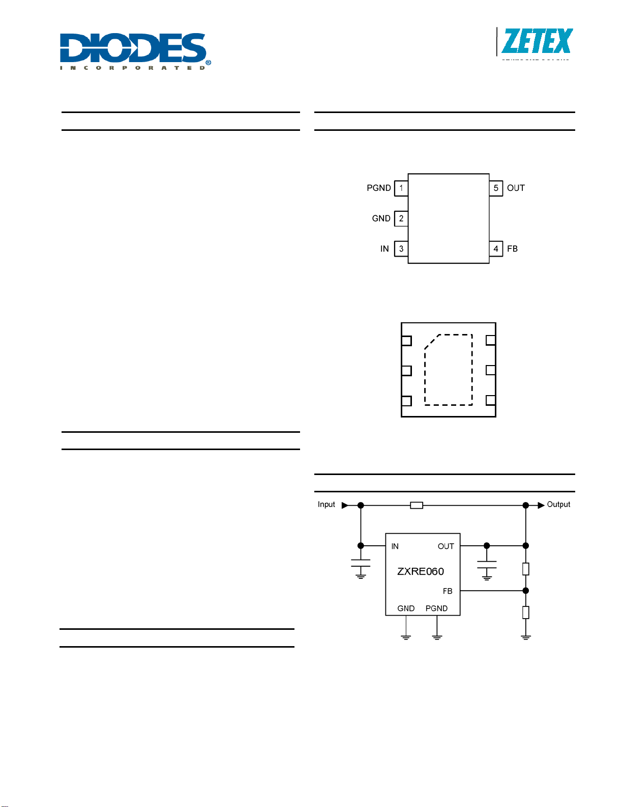
Pin Assignments
ZXRE060_H5 (SC70-5/SOT353) and ZXRE060_ET5
(TSOT23-5)
Top viewTop view
ZXRE060_FT4 (DFN1520H4-6)
Top view
Top view
6
PGND
PGND
1
1
6
5
N/C
N/C
2
2
5
OUT
OUT
3
3
4
4
Exposed flag floating or
Exposed flag floating or
connect to GND
connect to GND
Typical Application Circuit
IN
IN
GND
GND
FB
FB
Applications
• Isolated DC-DC converters
• Core voltage POL
• Low Voltage Low-Dropout linear regulators
• Shunt regulators
• Adjustable voltage reference
Notes: 1. No purposefully added lead.
2. Diodes Inc.’s “Green” policy can be found on our website at http://www.diodes.com/products/lead_free/index.php.
ZXRE060
Document number: DS33611 Rev. 6 - 2
1 of 12
www.diodes.com
March 2011
© Diodes Incorporated
A
f
Pin Description
Pin
(SC70-5 /SOT353,
TSOT23-5)
1 1 PGND
- 2 No connection
5 3 OUT
4 4 FB Feedback Input. Regulates to 600mV nominal.
2 5 GND
3 6 IN
- Flag Floating or connect to GND
Pin
(DFN)
Product Line o
Diodes Incorporated
ZXRE060
0.6V ADJUSTABLE PRECISION SHUNT REGULATOR
Name Function
Power Ground: Ground return for emitter of output transistor: Connect PGND and
GND together.
Output. Connect a capacitor close to device between OUT and GND. See the
Applications Information section.
Analog Ground: Ground return for reference and amplifier: Connect GND and
PGND together.
Supply Input. Connect a 0.1μF ceramic capacitor close to the device from IN to
GND.
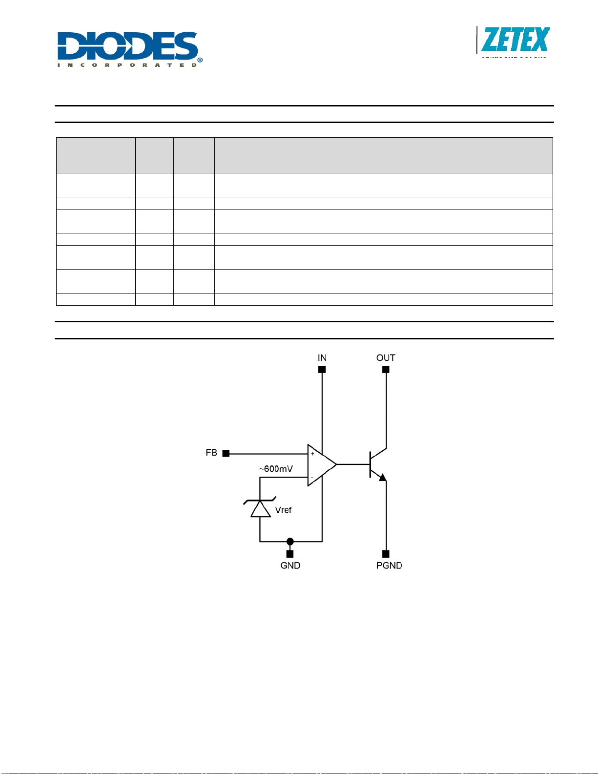
Function Block Diagram
The ZXRE060 differs from most other shunt regulators in that it has separate input a nd output pins and a low voltage reference.
This enables it to regulate rails down to 600mV and makes the part ideal for isolated power suppl y applications that use optocouplers in the feedback loop and where the open-collector output is required to operate down to voltages as low as 200mV.
The wide input voltage range of 2V to 18V and output volta ge range of 0.2V to 18V ena bles the ZXRE060 to be powered from
an auxiliary rail, while controlli ng a master rail which is above the auxiliar y rail voltage, or belo w the minimum V
allows it to operate as a low-dropout voltage regulator for microprocessor/DSP/PLD cores.
As with other shunt regulators (and shunt references), the ZXRE060 compares its internal amplifier FB pin to a high accurac y
internal reference; if FB is below the reference then OUT turns off, but if FB is above the reference then OUT sinks current – up
to a maximum of 15mA.
voltage. This
IN
ZXRE060
Document number: DS33611 Rev. 6 - 2
2 of 12
www.diodes.com
March 2011
© Diodes Incorporated
A
f
0.6V ADJUSTABLE PRECISION SHUNT REGULATOR
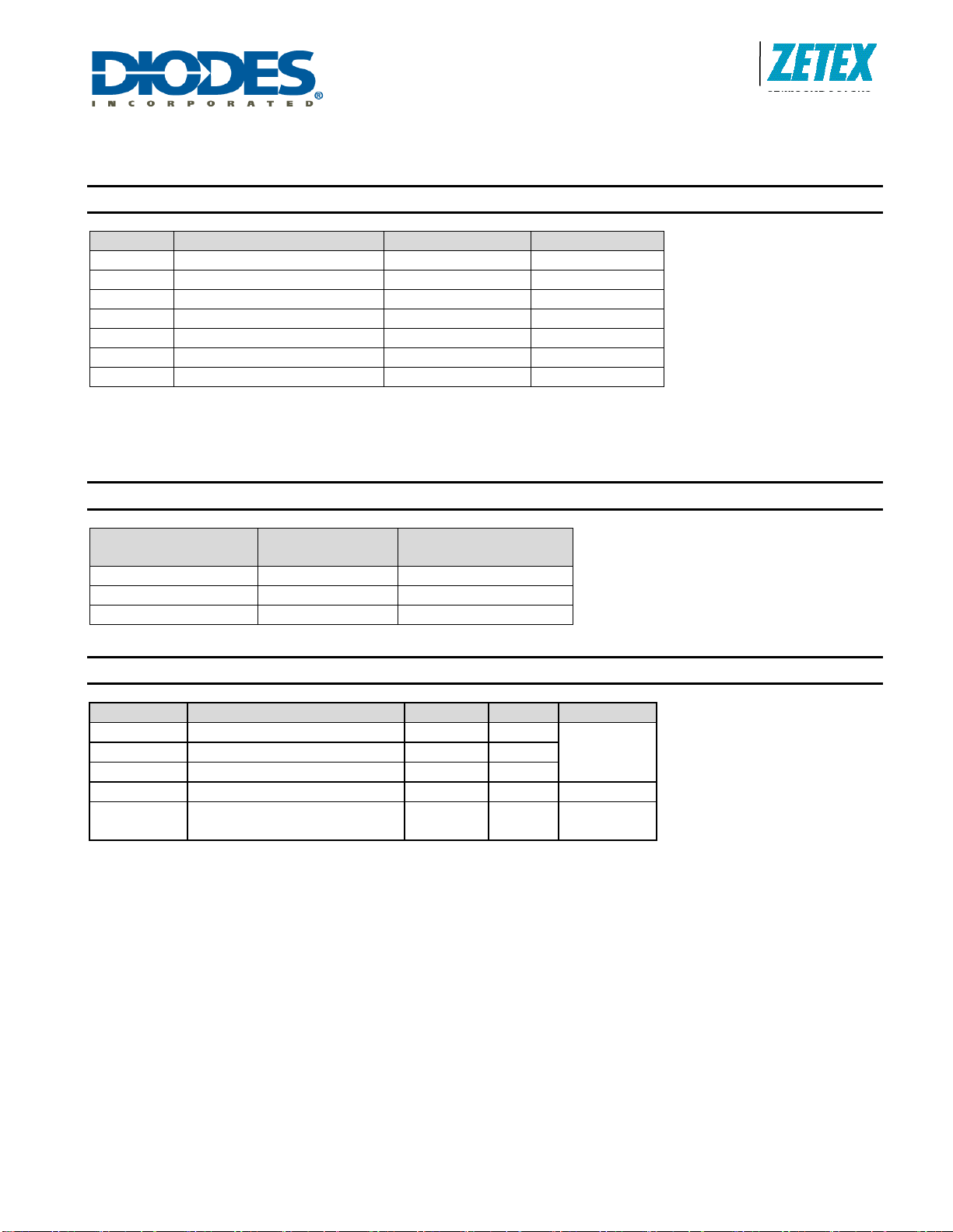
Absolute Maximum Ratings (Voltages to GND Unless Otherwise Stated)
Symbol Parameter Rating Unit
VIN IN Voltage relative to GND 20 V
V
OUT Voltage relative to GND 20 V
OUT
VFB FB Voltage relative to GND 20 V
P
PGND Voltage relative to GND -0.3 to +0.3 V
GND
I
OUT Pin Current 20 mA
OUT
TJ Operating Junction Temperture -40 to 150 °C
TST Storage Temperature 55 to 150 °C
These are stress ratings only. Operation outside the absolute maximum ratings may cause device failure.
Operation at the absolute maximum rating for extended periods may reduce device reliability.
Semiconductor devices are ESD sensitive and may be damaged by exposure to ESD events.
Suitable ESD precautions should be taken when handling and transporting these devices.
Package Thermal Data
P
Package θJA
TA = 25°C, TJ = 150°C
SC70-5/SOT353 400°C/W 310mW
TSOT23-5 250°C/W 500mW
DFN1520H4-6 TBD TBD
DIS
Product Line o
Diodes Incorporated
ZXRE060
Recommended Operating Conditions
Symbol Parameter Min Max Units
VIN IN Voltage Range (0 to 125°C) 2 18
VIN IN Voltage Range (-40 to 0°C) 2.2 18
V
OUT Voltage Range 0.2 18
OUT
I
OUT Pin Current 0.3 15 mA
OUT
TA
Operating Ambient Temperature
Range
ZXRE060
Document number: DS33611 Rev. 6 - 2
-40 125 °C
3 of 12
www.diodes.com
V
March 2011
© Diodes Incorporated
A
Product Line o
f
Diodes Incorporated
ZXRE060
0.6V ADJUSTABLE PRECISION SHUNT REGULATOR
Electrical Characteristics
= 25°C, VIN = 3.3V, V
T
A
Symbol Parameter Conditions Min Typ Max Units
VFB Feedback voltage
OUT
= VFB, I
= 5mA unless otherwise stated (Note 3).
OUT
TA = 0°C to 85°C
TA = -40°C to 85°C
ZXRE060A 0.597 0.6 0.603
ZXRE060 0.594 0.6 0.606
ZXRE060A 0.595 0.605
ZXRE060 0.592 0.608
ZXRE060A 0.594 0.606
ZXRE060 0.591 0.609
V
TA = -40°C to 125°C
ZXRE060A 0.593 0.607
ZXRE060 0.590 0.610
FB
FB
FB
LOAD
LINE
OVR
IFB
Feedback pin load
regulation
Feedback pin line
regulation
Output voltage
regulation
FB input bias
current
I
= 1 to 15mA
OUT
V
= 2V to 18V 0.1 1
IN
V
= 2.2V to 18V TA = -40 to 125°C 1.5
IN
V
= 0.2V to 18V,
OUT
I
=1mA
OUT
(Ref. Figure 1)
V
= 18V
IN
= 2V to 18V
V
IN
V
= 2.2V to 18V TA = -40 to 125°C 1
IN
I
OUT
=0.3mA
3.8 6
TA = -40 to 125°C 10
mV
mV
1
TA = -40 to 125°C
1.5
-45
TA = -40 to 125°C -200 0
mV
nA
0.35 0.7
mA
IIN Input current
V
= 2V to 18V
IN
V
= 2.2V to 18V TA = -40 to 125°C 1.5
IN
V
= 18V,
I
OUT(LK)
Z
PSRR
BW
Note: 3. Production testing of the device is performed at 25 °C. Functional operation of the device and parameters specified over the operating temperature
range are guaranteed by design, characterisation and process control.
OUT leakage
current
Dynamic Output
OUT
Impedance
Power supply
rejection ratio
Amplifier Unity Gain
Frequency
Amplifier
G
Transconductance
IN
V
= 18V,
OUT
V
=0V
FB
I
= 1 to 15mA
OUT
f < 1kHz
f=300kHz
V
= 0.3VPP
AC
Ref: Fig 2
I
OUT
=10mA
0.48 1
mA
0.1
TA = 125°C
1
0.25 0.4
TA = -40 to125°C 0.6
>45 dB
600 kHz
5000 mA/V
µA
Ω
ZXRE060
Document number: DS33611 Rev. 6 - 2
4 of 12
www.diodes.com
March 2011
© Diodes Incorporated
 Loading...