

Page 1
r
o
6
e
a
t
o
u
d
h
0
f
6
2
c
%
e
m
m
m
1
w
5
e
H
p
d
p
6
t
X
g
v
o
v
r
h
0
i
b
%
g
u
r
A
i
C
5
2
c
)
o
d
p
0
s
s
s
e
c
w
-
d
c
o
d
L
w
u
0
V
o
a
p
n
a
r
A
m
V
A
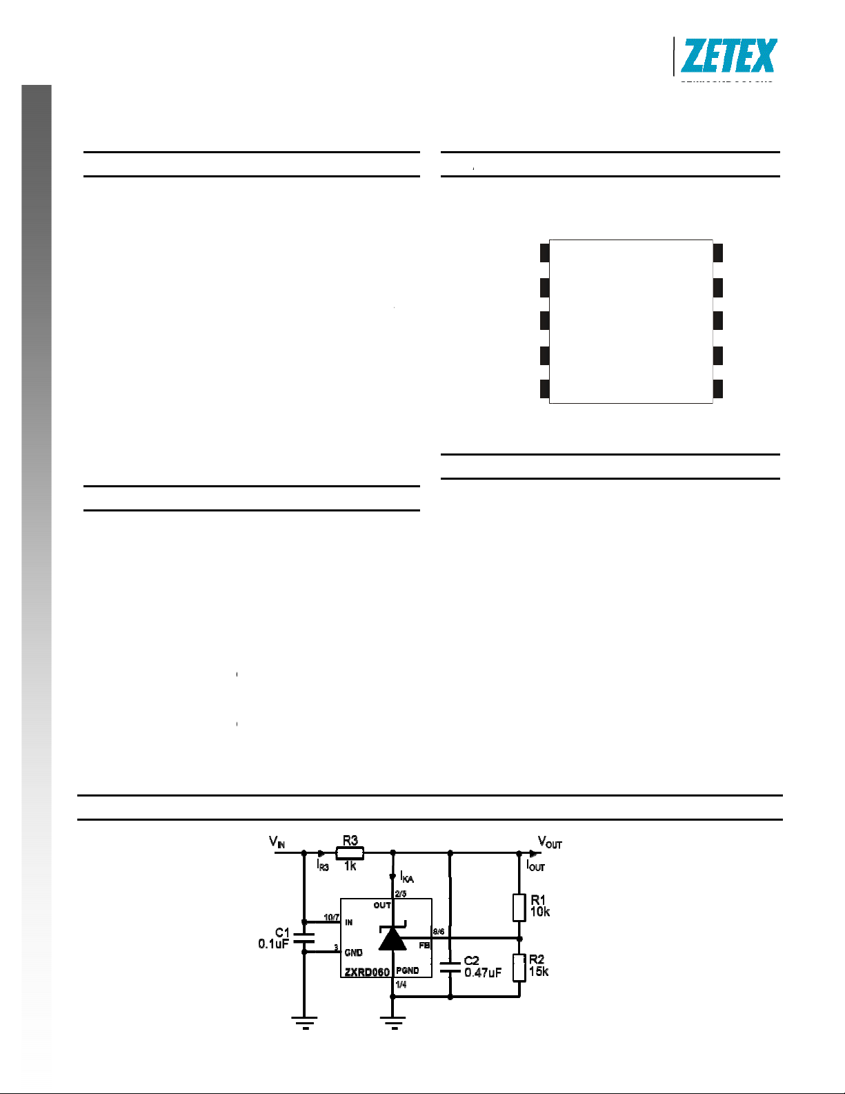
App
C• L• S• A
.
ADio
A
C
o
r
a
d
H
Product L
i
o
e
rs a
0
6
Z
G
o
f
des Incorp
ne o
rated
XRD060
.6V DUA
ADJUST
BLE PRE
CISION S
UNT RE
ULATOR
NEW PRODUCT
Descripti
The ZXRD0
regulator off
handling cap
isolated low
FB pin, it can
makes it ide
PLD core vol
The device
18V and reg
two external
Separating t
the ZXRD06
regulators op
The ZXRD0
tolerances o
respectively.
10 pin DFN2
Features
• Low refe
• -40 to 1
• Referen
o 0.5
o 1%
• Typical t
o <4
o <6
o <12
• 0.2V to
• High po
o (>4
• Lead Fr
• “Green”/
Notes: 1. No
2. Dio
n
0 is a 10-
ring excellent
ability. The Z
voltage DC-D
control the re
l for state of
age POL con
pen-collector
lated output
ivider resisto
e input from t
to be used
erating at low
60 is availa
0.5% and 1
It is available
26P10 packa
rence voltage
5ºC temperat
e voltage tole
ZXRD060
ZXRD060
mperature dr
V (0°C to 70°
V (-40°C to 8
V (-40°C to 1
8V open-colle
er supply reje
dB at 300kHz
e by design/R
alogen free
urposefully added
es Inc.’s “Green”
erminal adju
temperature
RD060 simpl
C regulators.
ulation of rail
the art microp
erters.
utput can op
oltage can be
s.
e open colle
to make lo
nput voltages.
le in two g
for the A an
in the space
e.
(VFB = 0.6V)
re range
ance at 25°C
ft
)
°C)
5°C)
tor output
ction
HS Complian
evice (Note 2)
lead.
olicy can be foun
table dual s
tability and o
ifies the desig
With its low
as low 0.6V.
rocessor/DSP
rate from 0.2
set by selecti
tor output en
cost low dro
rades with i
standard gr
saving low p
t (Note 1)
on our website at
Pin
hunt
tput
n of
.6V
This
and
to
n of
bles
-out
itial
des
ofile
• I
•
http://www.diodes
ssignme
PGND1
OUT1
GND
PGND2
OUT2
lications
solated DC-D
ore voltage P
ow Voltage L
hunt regulato
djustable volt
com/products/lea
nts
ZXRD
(DFN2
1
converters
OL
-Dropout lin
ge reference
_free/index.php.
60_FK
26P10)
ar regulators
IN1
N/C
FB1
IN2
FB2
Typical A
plication
Circuit
ZXRD060
Document numbe
: DS35359 Rev. 4
- 2
1 of 12
ww.diodes.co
August 2011
© Di
des Incorporated
Page 2
A
Product Line o
f
Diodes Incorporated
0.6V DUAL ADJUSTABLE PRECISION SHUNT REGULATOR
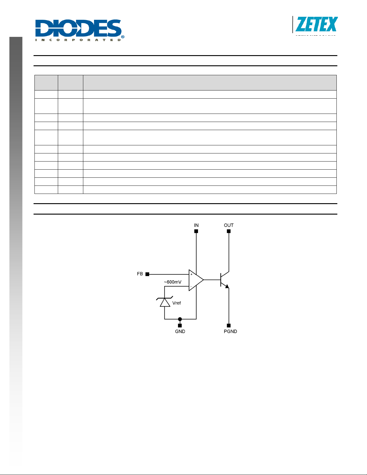
Pin Description
Pin
(DFN)
1 PGND1 Power Ground 1: Ground return for emitter of output transistor: Connect PGND1/2 and GND together.
2 OUT1
3 GND Analog Ground: Ground return for reference and amplifiers: Connect GND and PGND1/2 together.
4 PGND2 Power Ground 2: Ground return for emitter of output transistor: Connect PGND1/2 and GND together.
5 OUT2
6 FB2 Feedback Input 2. Regulates to 600mV nominal.
7 IN2 Supply Input 2. Connect a 0.1μF ceramic capacitor close to the device from IN2 to GND.
8 FB1 Feedback Input 1. Regulates to 600mV nominal.
9 No connection
10 IN1 Supply Input 1. Connect a 0.1μF ceramic capacitor close to the device from IN1 to GND.
Flag Floating or connect to GND
Name Function
Output 1. Connect a capacitor close to device between OUT1 and GND. See Applications Information
section.
Output 2. Connect a capacitor close to device between OUT2 and GND. See Applications Information
section.
ZXRD060
Function Block Diagram
NEW PRODUCT
The ZXRD060 differs from most other shunt regulators in that it has separate input and output pins and a low voltage
reference. This enables it to regulate rails do wn to 600mV and makes th e part idea l for is olated po wer suppl y applications that
use opto-couplers in the feedback loop and where the open-collect or output is required to op erate down to v oltages as lo w as
200mV.
The wide input voltage range of 2V to 18V and output voltage rang e of 0.2V to 1 8V enables the ZXRD060 to be po wered from
an auxiliary rail, while controlling a master rail which is above the auxi liary rail volt age, or belo w the minimum V
allows it to operate as a low-dropout voltage regulator for microprocessor/DSP/PLD cores.
As with other shunt regulators (and shunt references), the ZXRD060 c ompares its internal amplifier FB pin to a high accurac y
internal reference; if FB is below the reference then OUT turns off, but if FB is above the reference then OUT sinks current –
up to a maximum of 15mA.
ZXRD060
Document number: DS35359 Rev. 4 - 2
2 of 12
www.diodes.com
voltage. This
IN
August 2011
© Diodes Incorporated
Page 3
A
Product Line o
f
Diodes Incorporated
0.6V DUAL ADJUSTABLE PRECISION SHUNT REGULATOR
Absolute Maximum Ratings (Voltages to GND Unless Otherwise Stated)
Symbol Parameter Rating Unit
VIN IN Voltage relative to GND 20 V
V
OUT Voltage relative to GND 20 V
OUT
VFB FB Voltage relative to GND 20 V
P
PGND Voltage relative to GND -0.3 to +0.3 V
GND
I
OUT Pin Current 20 mA
OUT
TJ Operating Junction Temperture -40 to 150 °C
TST Storage Temperature 55 to 150 °C
Stresses greater than the 'Absolute Maximum Ratings' specified above, may cause permanent damage to the device. These are stress ratings only; functional
operation of the device at these or any other conditions exceeding those indicated in this specification is not implied. Device reliability may be affected by exposure
to absolute maximum rating conditions for extended periods of time.
Semiconductor devices are ESD sensitive and may be damaged by exposure to ESD events. Suitable ESD precautions should be taken when handling and
transporting these devices.
Package Thermal Data
P
DIS
NEW PRODUCT
Package θJA
TA = 25°C, TJ = 150°C
DFN2626P10 152°C/W 0.8W
ZXRD060
Recommended Operating Conditions
Symbol Parameter Min Max Units
VIN IN Voltage Range (0 to 125°C) 2 18
VIN IN Voltage Range (-40 to 0°C) 2.2 18
V
OUT Voltage Range 0.2 18
OUT
I
OUT Pin Current 0.3 15 mA
OUT
TA Operating Ambient Temperatu r e Range -40 125 °C
V
ZXRD060
Document number: DS35359 Rev. 4 - 2
3 of 12
www.diodes.com
August 2011
© Diodes Incorporated
Page 4
A
Product Line o
f
Diodes Incorporated
ZXRD060
0.6V DUAL ADJUSTABLE PRECISION SHUNT REGULATOR
Electrical Characteristics
= 25°C, VIN = 3.3V, V
T
A
Symbol Parameter Conditions Min Typ Max Units
VFB Feedback voltage
OUT
= VFB, I
= 5mA unless otherwise stated (Note 3).
OUT
TA = 0°C to 85°C
TA = -40°C to 85°C
ZXRD060A 0.597 0.6 0.603
ZXRD060 0.594 0.6 0.606
ZXRD060A 0.595 0.605
ZXRD060 0.592 0.608
ZXRD060A 0.594 0.606
ZXRD060 0.591 0.609
V
TA = -40°C to 125°C
ZXRD060A 0.593 0.607
ZXRD060 0.590 0.610
3.8 6
TA = -40 to 125°C 10
mV
mV
1
TA = -40 to 125°C
1.5
-45
TA = -40 to 125°C -200 0
mV
nA
0.35 0.7
mA
NEW PRODUCT
FB
FB
FB
LOAD
LINE
OVR
IFB
Feedback pin load
regulation
Feedback pin line
regulation
Output voltage
regulation
FB input bias
current
I
= 1 to 15mA
OUT
= 2V to 18V 0.1 1
V
IN
V
= 2.2V to 18V TA = -40 to 125°C 1.5
IN
= 0.2V to 18V,
V
OUT
=1mA
I
OUT
(Ref. Figure 1)
VIN = 18V
V
= 2V to 18V
IN
V
= 2.2V to 18V TA = -40 to 125°C 1
IN
I
OUT
=0.3mA
IIN Input current
V
= 2V to 18V
IN
V
= 2.2V to 18V TA = -40 to 125°C 1.5
IN
= 18V,
V
I
OUT(LK)
Z
PSRR
BW
Note: 3. Production testing of the device is performed at 25°C. Functional operation of the device and parameters specified over the operating temperature
range are guaranteed by design, characterisation and process control.
OUT leakage
current
Dynamic Output
OUT
Impedance
Power supply
rejection ratio
Amplifier Unity Gain
Frequency
Amplifier
G
Transconductance
IN
= 18V,
V
OUT
=0V
V
FB
I
= 1 to 15mA
OUT
f < 1kHz
f = 300kHz
= 0.3VPP
V
AC
Ref: Fig 2
I
OUT
=10mA
0.48 1
mA
0.1
TA = 125°C
1
0.25 0.4
TA = -40 to125°C 0.6
>45 dB
600 kHz
5000 mA/V
µA
Ω
ZXRD060
Document number: DS35359 Rev. 4 - 2
4 of 12
www.diodes.com
August 2011
© Diodes Incorporated
Page 5

A
f
Typical Characteristics
Product Line o
Diodes Incorporated
ZXRD060
0.6V DUAL ADJUSTABLE PRECISION SHUNT REGULATOR
NEW PRODUCT
ZXRD060
Document number: DS35359 Rev. 4 - 2
5 of 12
www.diodes.com
August 2011
© Diodes Incorporated
Page 6

A
f
T
T
OU
OU
0.6V DUAL ADJUSTABLE PRECISION SHUNT REGULATOR
Typical Operating Conditions (cont.)
200
200
150
150
V
= 0.6V
V
= 0.6V
OUT
OUT
C
C
= 2.2uF
= 2.2uF
OUT
OUT
100
100
Gain (dB)
Gain (dB)
50
50
0
0
Gain
Gain
Gain
Phase
Phase
Phase
-50
-50
1 10 100 1k 10k 100k 1M
1 10 100 1k 10k 100k 1M
Gain and Phase vsFrequency, V
Gain and Phase vsFrequency, V
Frequency (Hz)
Frequency (Hz)
OU
OU
=0.6V
=0.6V
225
225
180
180
135
135
90
90
45
45
0
0
Product Line o
Diodes Incorporated
ZXRD060
200
200
150
150
V
V
C
C
OUT
OUT
OUT
OUT
= 6V
= 6V
= 0.22uF
= 0.22uF
225
225
180
180
100
100
135
135
Gain (dB)
Gain (dB)
50
50
Phase (deg)
Phase (deg)
0
0
Gain
Gain
Gain
Phase
Phase
-50
-50
Phase
1 10 100 1k 10k 100k 1M
1 10 100 1k 10k 100k 1M
Gain and Phase vsFrequency , V
Gain and Phase vsFrequency , V
Frequency (Hz)
Frequency (Hz)
T
T
=6V
=6V
90
90
Phase (deg)
Phase (deg)
45
45
0
0
NEW PRODUCT
50Ω
50Ω
Fig. 2 Test Circuits for Gain and Phase Plots
ZXRD060
Document number: DS35359 Rev. 4 - 2
6 of 12
www.diodes.com
August 2011
© Diodes Incorporated
Page 7

NEW PRODUCT
r
o
o
C
n
i
n
n
n
b
n
h
a
y
a
U
V
S
U
r
o
e
e
r
=
0
y
t
y
a
e
o
a
e
h
y
e
B
L
w
e
s
e
y
a
A
m
D
e
o
i
ff
w
ADio
o
d
2
o
V
1
0
n
i
H
i
o
p
o
+
U
R
D
K
N
l
Z
G
o
f
t
t
l
t
Applicati
The following
capacitor C2 t
formed by C2
Both C1 and
case of fig 9 a
F
ns Inform
show some t
guarantee st
and R3 should
2 should be
d fig10, it me
V
O
3R =
Fig.3 0.6V
V
g.5 0.6V Se
tion
pical applica
ability. C2 ma
be greater th
as close to th
ns the opto-c
VT=
REF
−
V
OUT
IN
I
3R
hunt Regul
VT=
O
REF
ies LDO reg
.6V DUA
ion examples
range in valu
n 1ms multipli
ZXRD060 a
upler will hav
tor
ulator
Product L
des Incorp
ne o
rated
XRD060
ADJUST
for the ZXR
from 0.1µF t
ed by the feed
possible and
to be carefull
BLE PRE
060. It is rec
10µF depen
back factor R
connected to
y positioned t
Fig.4
CISION S
mmended to
ing on the ap
/(R1 + R2).
it with the sh
enable this.
= 1
V
OUT
REF
V
V3R−
IN
=
I
.0V Shunt
3R
UNT RE
include the c
lication. The
rtest possible
1R
⎛
⎞
⎜
⎟
2R
⎝
⎠
T
O
egulator
ULATOR
ompensation
ime constant
track. In the
1R
⎛
⎞
+= 1
V
Fig.6 1.
V
OUT
V Series L
REF
⎜
⎝
⎟
2R
⎠
O regulator
Design gui
1. Determi
2. Determi
3. Determi
conventi
necessa
should
4. Determi
5. Althoug
ZXRD060
Document numbe
de
e I
and ch
OUT
e IB from
e IR3 from
onal referenc
ry to determin
e adequate fo
e R3 from
unlikely to be
: DS35359 Rev. 4
ose a suitabl
I
I =
B
(
h
(min)FE
I
3R
s. There is onl
an I
this.
3R
a problem, en
- 2
(max)OUT
IBI +≥
(min)KA
KA(min)
V(INV +−
+
OUT
I
)1
. T
to
3R
transistor taki
e design of th
an output le
nsure that the
V
)
.
E
sure that I
ng power diss
e ZXRD060 e
kage current
device operat
15 mA.
≤
R3
ww.diodes.co
7 of 12
pation into co
ectively mean
hich is a max
es within its lin
sideration.
s there is no I
mum of 1µA.
ear range at a
limitation
A(min)
evertheless, i
l times. I
KA(min)
© Di
as in
is
≥ 10µA
August 2011
des Incorporated
Page 8

NEW PRODUCT
r
o
i
i
i
i
s
t
8
a
r
h
3
R
t
t
=
r
0
.
e
e
a
a
d
L
w
g
e
k
n
m
A
m
s
f
a
+
o
ADio
=
e
w
r
H
i
o
i
s
o
Z
G
o
f
o
0
Applicati
Design gu
1. Determ
2. Determ
3. Determ
4. Determ
5. It is be
minimis
<15mA
6. Calcula
Fig.
ns Inform
Fig.7 1V Cu
ide
ne I
and c
OUT
ne IB from
ne IR3 from
ne R3 from
t to let the ZX
e the strain on
for this curren
e R4 from
1.15V Ove
I =
B
I
tion
(cont
rent-Boost
oose a suitabl
I
(max)OUT
h(
+
(min)FE
I=
3R
(max)OUT
−
V
V
OUT
IN
=
R
I
3R
D060 supply
Q1, it also gu
, IR4.
V
BE
4R
I
4R
-Voltage In
)
d Shunt Re
)1
s much curre
rantees the
icator
.6V DUA
transistor ta
ADJUST
ulator
ing power dis
t as it can be
ost stable ope
V
goes low
OUT
⎛
> 1
V
V
M
and IF are f
V
F
=
REF
V3R−
IN
ImA15 ≤≥
⎜
⎝
V(
I
3R
BLE PRE
V
(
ipation into co
ore bringing Q
ration. Choos
nd LED1 is lit
1R
⎞
⎟
2R
⎠
)2.0+
F
3R
I
)MAX(F
rward voltage d
Product L
des Incorp
CISION S
V
REF
OUT
V
OUT
V
I
3R =
I
nsideration.
1 into conduct
a nominal val
hen monitored
op and current
VN−
3R
⎛
⎜
⎝
OUT
ne o
rated
XRD060
UNT RE
1R
⎞
+
1
⎟
2R
⎠
)
VV2.0 +≥
BE
ULATOR
on. Not only d
ue between 1
upply
f LED1.
es this
mA and
ZXRD060
Document numbe
: DS35359 Rev. 4
- 2
8 of 12
ww.diodes.co
August 2011
© Di
des Incorporated
Page 9

NEW PRODUCT
r
o
o
o
n
n
n
n
n
n
a
U
t
o
e
n
e
e
e
e
e
e
0
.
u
w
n
L
w
r
s
l
u
l
h
c
o
A
m
h
w
o
o
g
ADio
1
e
u
g
H
i
o
F
.
Z
G
o
f
e
Applicati
Fig.9
VF and IF are f
More applicati
AN58 - Desig
AN59 - Desig
AN60 - Desig
AN61 - Desig
AN62 - Desig
AN63 - Desig
ns Inform
mA15 ≥
3R =
V
Opto-Isola
rward voltag
ns informatio
ing with Diod
ing with Diod
ing with Diod
ing with Diod
ing with Diod
ing with Diod
tion
(cont
I
I ≤
3R
V
V(N+−
I
F
I
3R
VT=
O
REF
ed 0.6V Sh
drop and for
is available i
s’ References
s’ References
s’ References
s’ References
s’ References
s’ References
)
)MAX(F
)2.0
nt Regulato
ard current re
the following
– Shunt Regu
– Series Reg
– Fixed Regu
– Extending t
– Other Appli
– ZXRE060 L
.6V DUA
ADJUST
pectively for t
publications
ation
lation
ators and Opt
e operating v
ations
w Voltage Re
BLE PRE
Fig. 10 Opt
e opto-coupl
hich can be fo
-Isolation
ltage range
ulator
Product L
des Incorp
CISION S
ImA
5 ≤≥
V
OUT
=
V3R−
3R
V(
IN
I
= 1
V
REF
o-Isolated 1
r LED.
nd on Diodes
ne o
rated
UNT RE
I
)MAX(
)2.0+
F
3R
1R
⎛
⎞
+
⎜
⎟
2R
⎝
⎠
0V Shunt R
’ web site.
XRD060
ULATOR
gulator
ZXRD060
Document numbe
: DS35359 Rev. 4
- 2
9 of 12
ww.diodes.co
August 2011
© Di
des Incorporated
Page 10

A
Product Line o
f
Diodes Incorporated
0.6V DUAL ADJUSTABLE PRECISION SHUNT REGULATOR
Ordering Information
Tolerance Package Packing
Tolerance Package Packing
A: ±0.5%
A: ±0.5%
None: ±1%
None: ±1%
XXXZXRD060
XXXZXRD060
Package Packing
Package
FK: DFN2626P10
FK: DFN2626P10
Tol. Order Code Part
0.5% ZXRD060AFK-7 DFN2626P10 S6A 7”, 180mm 8mm 3000
1% ZXRD060FK-7 DFN2626P10 S06 7”, 180mm 8mm 3000
For packaging details, go to our website at http://www.diodes.com/datasheets/ap02007.pdf
XX
XX
Identification
Code
Packing
-7: Tape & Reel
-7: Tape & Reel
Reel Size Tape Width Quantity/Reel
ZXRD060
Marking Information
DFN2626P10
NEW PRODUCT
Top V iew
Top V iew
6
6
6
6
6
6
5
5
5
9
5
5
5
9
52
52
54
7
52
52
54
10
10
1
1
1
1
1
1
1
1
7
XXX
XXX
WX
WX
Y
Y
34
34
34
38
34
34
34
38
2
2
2
2
2
2
2
2
2
2
XXX : Identification code
XXX : Identification code
Y : Year : 0~9
Y : Year : 0~9
W
W
: Week : A~Z : 1~26 we ek ;
: Week : A~Z : 1~26 we ek ;
a~z : 27~52 week;
a~z : 27~52 week;
z : represents 52 and 53
z : represents 52 and 53
: A~Z : Internal Code
: A~Z : Internal Code
X
X
34
34
34
5 6
34
34
34
5 6
ZXRD060
Document number: DS35359 Rev. 4 - 2
10 of 12
www.diodes.com
August 2011
© Diodes Incorporated
Page 11

A
f
0.6V DUAL ADJUSTABLE PRECISION SHUNT REGULATOR
Package Outline Dimensions (All Dimensions in mm)
DFN2626P10
NEW PRODUCT
Product Line o
Diodes Incorporated
ZXRD060
ZXRD060
Document number: DS35359 Rev. 4 - 2
11 of 12
www.diodes.com
August 2011
© Diodes Incorporated
Page 12

A
Product Line o
f
Diodes Incorporated
0.6V DUAL ADJUSTABLE PRECISION SHUNT REGULATOR
DIODES INCORPORATED MAKES NO WARRANTY OF ANY KIND, EXPRESS OR IMPLIED, WITH REGARDS TO THIS DOCUMENT,
INCLUDING, BUT NOT LIMITED TO, THE IMPLIED WARRANTIES OF MERCHANTABILITY AND FITNESS FOR A PARTICULAR PURPOSE
(AND THEIR EQUIVALENTS UNDER THE LAWS OF ANY JURISDICTION).
Diodes Incorporated and its subsidiaries reserve the right to make modifications, enhancements, improvements, corrections or other changes
without further notice to this document and any product described herein. Diodes Incorporated does not assume any liability arising out of the
application or use of this document or any product described herein; neither does Diodes Incorporated convey any license under its patent or
trademark rights, nor the rights of others. Any Customer or user of this document or products described herein in such applications shall assume
all risks of such use and will agree to hold Diodes Incorporated and all the companies whose products are represented on Diodes Incorporated
website, harmless against all damages.
Diodes Incorporated does not warrant or accept any liability whatsoever in respect of any products purchased through unauthorized sales
channel.
Should Customers purchase or use Diodes Incorporated products for any unintended or unauthorized application, Customers shall indemnify and
hold Diodes Incorporated and its representatives harmless against all claims, damages, expenses, and attorney fees arising out of, directly or
indirectly, any claim of personal injury or death associated with such unintended or unauthorized application.
Products described herein may be covered by one or more United States, international or fo reign p atents pending. Product names a nd markings
noted herein may also be covered by one or more United States, international or foreign trademarks.
Diodes Incorporated products are specifically not authorized for use as critical components in life support devices or systems without the express
written approval of the Chief Executive Officer of Diodes Incorporated. As used herein:
A. Life support devices or systems are devices or systems which:
NEW PRODUCT
1. are intended to implant into the body, or
labeling can be reasonably expected to result in significant injury to the user.
B. A critical component is any component in a life support device or system whose failure to perform can be reasonably expected to cause the
failure of the life support device or to affect its safety or effectiveness.
Customers represent that they have all necessary expertise in the safety and regulatory ramifications of their life support devices or systems, and
acknowledge and agree that they are solely responsible for all legal, regulatory and safety-related requirements concerning their products and
any use of Diodes Incorporated products in such safety-critical, life support devices or systems, notwithstanding any devices- or systems-related
information or support that may be provided by Diodes Incorporated. Further, Customers must fully indemnify Diodes Incorporated and its
representatives against any damages arising out of the use of Diodes Incorporated products in such safety-critical, life support devices or
systems.
Copyright © 2011, Diodes Incorporated
www.diodes.com
2. support or sustain life and whose failure to perform when properly used in accordance with instructions for use provided in the
IMPORTANT NOTICE
LIFE SUPPORT
ZXRD060
ZXRD060
Document number: DS35359 Rev. 4 - 2
12 of 12
www.diodes.com
August 2011
© Diodes Incorporated
 Loading...