

Page 1
f
60V N-CHANNEL SELF PROTECTED ENHANCEMENT MODE
Product Summary
• Continuos drain source voltage 60V
• On-state resistance 100mΩ
• Nominal load current (VIN = 5V) 2.8A
• Clamping Energy 490mJ
Description and Applications
The ZXMS6006DG is a self protected low side MOSFET with logic
level input. It integrates over-temperature, over-current, over-voltage
(active clamp) and ESD protected logic level functionality. The
ZXMS6006DG is ideal as a general purpose switch driven from 3.3V
or 5V microcontrollers in harsh environments where standard
MOSFETs are not rugged enough.
ADVANCE INFORMATION
• Lamp Driver
• Motor Driver
• Relay Driver
• Solenoid Driver
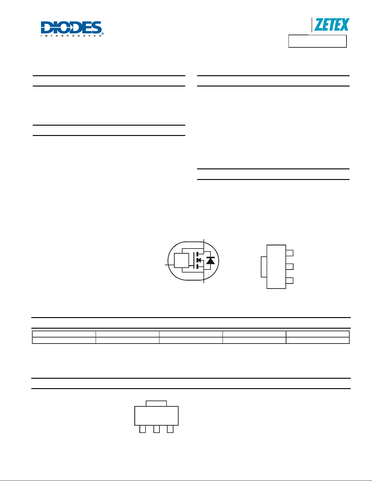
SOT-223
Top View
IN
Features and Benefits
• Compact high power dissipation package
• Low input current
• Logic Level Input (3.3V and 5V)
• Short circuit protection with auto restart
• Over voltage protection (active clamp)
• Thermal shutdown with auto restart
• Over-current protection
• Input Protection (ESD)
• High continuous current rating
• Green, RoHS Compliant (Note 1)
• Halogen and Antimony Free. (Note 2)
• Qualified to AEC-Q101 Standards for High Reliability
Mechanical Data
• Case: SOT-223
• Case Material: Molded Plastic, “Green” Molding Compound.
• Moisture Sensitivity: Level 1 per J-STD-020
• Terminals: Matte Tin Finish
• Weight: 0.112 grams (approximate)
Device symbol
A Product Line o
Diodes Incorporated
INTELLIFET
UL Flammability Classification Rating 94V-0
D
D
S
Top view
Pin Out
ZXMS6006DG
®
MOSFET
S
D
IN
Ordering Information (Note 3)
Product Marking Reel size (inches) Tape width (mm) Quantity per reel
ZXMS6006DGTA ZXMS6006D 7 12 1,000
Notes: 1. Contain <900ppm bromine, chlorine (<1500ppm total) and <1000ppm antimony compounds.
3. For packaging details, go to our website at http://www.diodes.com
2. Diodes Inc’s “Green” Policy can be found on our website at http://www.diodes.com
Marking Information
IntelliFET® is a trademark of Diodes Incorporated, registered in the United States and other jurisdictions worldwide.
ZXMS6006DG
Document number: DS35142 Rev. 1 - 2
ZXMS
6006D
ZXMS6006D = Product type Marking Code
1 of 9
www.diodes.com
December 2010
© Diodes Incorporated
Page 2
f
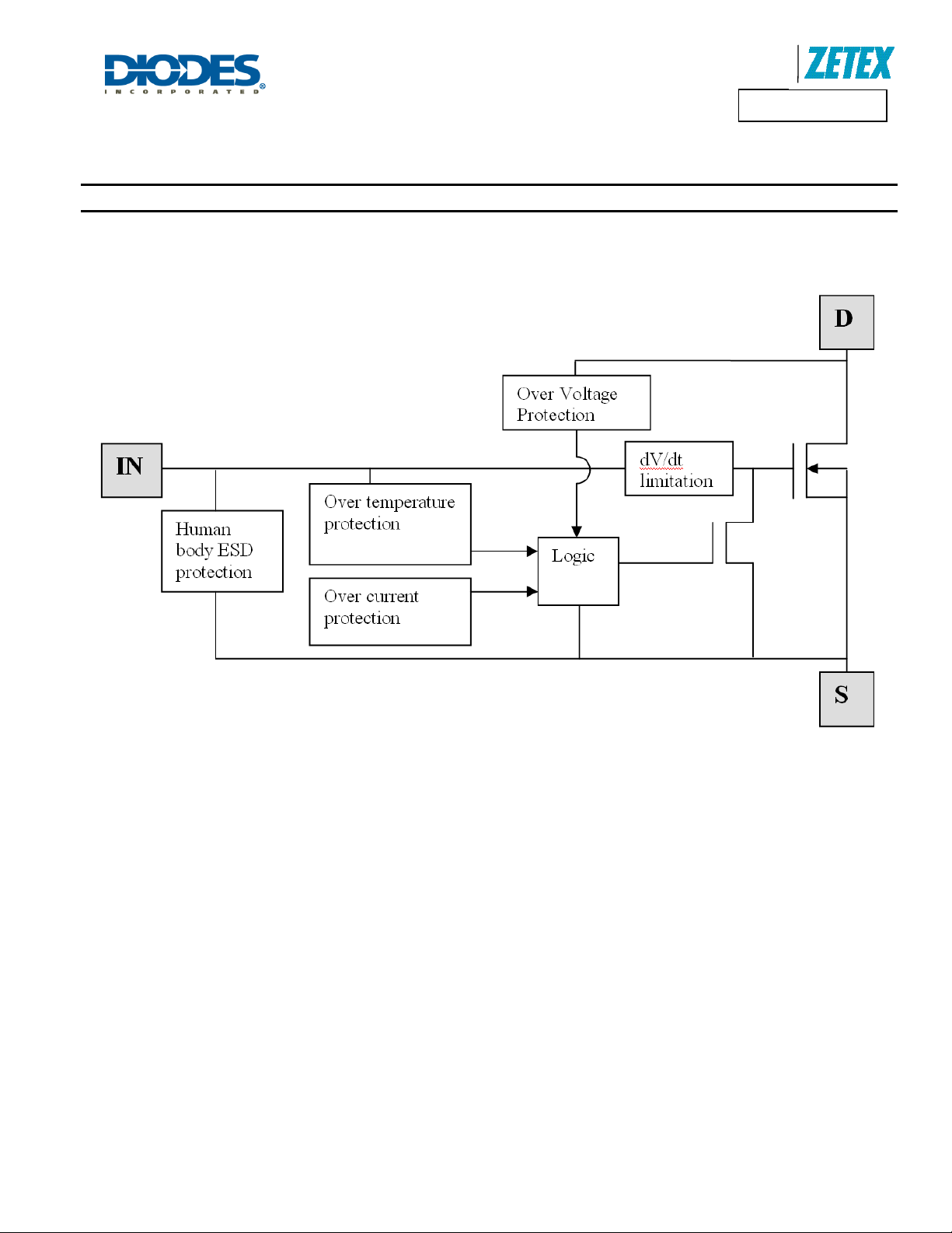
Functional Block Diagram
ADVANCE INFORMATION
A Product Line o
Diodes Incorporated
ZXMS6006DG
IntelliFET® is a trademark of Diodes Incorporated, registered in the United States and other jurisdictions worldwide.
ZXMS6006DG
Document number: DS35142 Rev. 1 - 2
2 of 9
www.diodes.com
December 2010
© Diodes Incorporated
Page 3
f
)
A Product Line o
Diodes Incorporated
ZXMS6006DG
Maximum Ratings @T
= 25°C unless otherwise specified
A
Characteristic Symbol Value Units
Continuous Drain-Source Voltage
Drain-Source Voltage for Short Circuit Protection
Continuous Input Voltage
Continuous Input Current @-0.2V ≤ VIN ≤ 6V
Continuous Input Current @V
< -0.2V or VIN > 6V
IN
V
DS(SC
V
DS
V
IN
I
IN
Pulsed Drain Current @VIN = 3.3V IDM
Pulsed Drain Current @VIN = 5V IDM
Continuous Source Current (Body Diode) (Note 4)
Pulsed Source Current (Body Diode)
Unclamped Single Pulse Inductive Energy,
= 25°C, ID = 0.5A, VDD = 24V
T
J
Electrostatic Discharge (Human Body Model)
Charged Device Model
ADVANCE INFORMATION
V
V
I
E
ESD
CDM
I
SM
S
AS
Thermal Characteristics @T
= 25°C unless otherwise specified
A
Characteristic Symbol Value Units
Power Dissipation at TA = 25°C (Note 4)
Linear Derating Factor
Power Dissipation at TA = 25°C (Note 5)
Linear Derating Factor
Thermal Resistance, Junction to Ambient (Note 4)
Thermal Resistance, Junction to Ambient (Note 5)
Thermal Resistance, Junction to Case (Note 6)
Operating Temperature Range
Storage Temperature Range
Notes: 4. For a device surface mounted on 15mm x 15mm single sided 1oz weight copper on 1.6mm FR4 board, in still air conditions.
5. For a device surface mounted on 50mm x 50mm single sided 2oz weight copper on 1.6mm FR4 board, in still air conditions.
6. Thermal resistance between junction and the mounting surfaces of drain and source pins.
P
D
P
D
R
θJA
R
θJA
R
θJC
T
J
T
STG
-40 to +150
-55 to +150
60 V
16 V
-0.5 ... +6 V
No limit
│≤2
│I
IN
mA
11 A
13 A
2 A
12 A
490 mJ
4000 V
1000 V
1.3
10.4
3.0
24
96
42
12
W
mW/°C
W
mW/°C
°C/W
°C/W
°C/W
°C
°C
IntelliFET® is a trademark of Diodes Incorporated, registered in the United States and other jurisdictions worldwide.
ZXMS6006DG
Document number: DS35142 Rev. 1 - 2
3 of 9
www.diodes.com
December 2010
© Diodes Incorporated
Page 4

f
Recommended Operating Conditions
The ZXMS6006DG is optimized for use with µC operating from 3.3V and 5V supplies.
Characteristic Symbol Min Max Unit
Input Voltage Range
Ambient Temperature Range
High Level Input Voltage for MOSFET to be on
Low level input voltage for MOSFET to be off
Peripheral Supply Voltage (voltage to which load is referred)
Thermal Characteristics
ADVANCE INFORMATION
A Product Line o
Diodes Incorporated
ZXMS6006DG
V
IN
T
A
V
IH
V
IL
V
P
0 5.5 V
-40 125 °C
3 5.5 V
0 0.7 V
0 16 V
Limited by Over-Current Protection
DC
1s
100ms
10ms
Limit of s/c protection
110
10
100m
Drain Current (A)
D
10m
I
Limited
by R
DS(on)
1
Single Pulse
T
=25°C
amb
15X15X1.6 mm
Single 1oz FR4
VDS Drain-Source Voltage (V)
Safe Operating Area
100
Thermal Resistance (°C/W)
15X15X1.6 mm
90
Single 1oz FR4
80
70
60
50
40
30
20
10
T
=25°C
amb
D=0.5
D=0.2
0
100µ 1m 10m 100m 1 10 100 1k
D=0.1
Single Pulse
D=0.05
Pulse Width (s)
Transient Thermal Impedance
1ms
3.0
2.5
2.0
1.5
1.0
0.5
0.0
Max Power Dissipation (W)
15X15X1.6 mm
Single 1oz FR4
0 25 50 75 100 125 150
50X50X1.6 mm
Single 2oz FR4
Temperature (°C)
Derating Curve
100
10
Maximum Power (W)
1
100µ 1m 10m 100m 1 10 100 1k
Pulse Width (s )
15X15X1.6 mm
Single 1oz FR4
Single Pulse
T
=25°C
amb
Pulse Power Dissipation
IntelliFET® is a trademark of Diodes Incorporated, registered in the United States and other jurisdictions worldwide.
ZXMS6006DG
Document number: DS35142 Rev. 1 - 2
4 of 9
www.diodes.com
December 2010
© Diodes Incorporated
Page 5

f
)
)
)
r
)
A Product Line o
Diodes Incorporated
ZXMS6006DG
Electrical Characteristics @T
= 25°C unless otherwise specified
A
Characteristic Symbol Min Typ Max Unit Test Condition
Static Characteristics
Drain-Source Clamp Voltage
Off State Drain Current
Input Threshold Voltage
Input Current
V
V
DS(AZ
I
DSS
IN(th
I
IN
Input Current While Over Temperature Active - - - 400
Static Drain-Source On-State Resistance
R
DS(on)
Continuous Drain Current (Note 4)
I
I
D(LIM)
D
ADVANCE INFORMATION
Continuous Drain Current (Note 5)
Current Limit (Note 7)
60 65 70 V
- - 1
- - 2
0.7 1 1.5 V
- 60 100
- 120 200
- 85 125
- 75 100
2.0 - -
2.2 - -
2.6 - -
2.8 - 4 8 6 13 -
µA
μA
μA
mΩ
A
A
ID = 10mA
= 12V, VIN = 0V
V
DS
V
= 36V, VIN = 0V
DS
VDS = VGS, ID = 1mA
= +3V
V
IN
V
= +5V
IN
= +5V
V
IN
= +3V, ID = 1A
V
IN
V
= +5V, ID = 1A
IN
= 3V; TA = 25°C
V
IN
V
= 5V; TA = 25°C
IN
V
= 3V; TA = 25°C
IN
V
= 5V; TA = 25°C
IN
= +3V
V
IN
V
= +5V
IN
Dynamic Characteristics
Turn On Delay Time
Rise Time
Turn Off Delay Time
Fall Time
t
t
d(on
d(off
t
f
f
- 8.6 -
- 18 -
- 34 -
- 15 -
μs
V
= 12V, ID = 1A, VGS = 5V
DD
Over-Temperature Protection
Thermal Overload Trip Temperature (Note 8)
Thermal Hysteresis (Note 8)
Notes: 7. The drain current is restricted only when the device is in saturation (see graph ‘typical output characteristic’). This allows the device to be used in the fully
on state without interference from the current limit. The device is fully protected at all drain currents, as the low power dissipation generated outside
saturation makes current limit unnecessary.
8. Over-temperature protection is designed to prevent device destruction under fault conditions. Fault conditions are considered as “outside” normal
operating range, so this part is not designed to withstand over-temperature for extended periods..
T
JT
f
f
150 175 -
- 10 -
°C
°C
-
-
IntelliFET® is a trademark of Diodes Incorporated, registered in the United States and other jurisdictions worldwide.
ZXMS6006DG
Document number: DS35142 Rev. 1 - 2
5 of 9
www.diodes.com
December 2010
© Diodes Incorporated
Page 6

f
Typical Characteristics
Drain Current (A)
D
I
ADVANCE INFORMATION
16
14
12
10
8
6
4
2
0
0123456789101112
TA = 25°C
VDS Drain-Source Voltage (V)
Typical Output Ch aracteristic
V
IN
5V
4.5V
4V
3.5V
3V
3V
2.5V
2V
A Product Line o
Diodes Incorporated
ZXMS6006DG
120
100
80
60
40
20
Input Current (μA)
IN
I
0
012345
VIN Input Voltage (V)
Input Cu rrent vs Input V oltage
0.20
0.15
0.10
On-Resistance (Ω)
0.05
DS(on)
R
0.00
2.0 2.5 3.0 3.5 4.0 4.5 5.0
TJ = 150°C
TJ = 25°C
VIN Input Voltage (V)
On-Resistance vs Input Voltage
0.20
0.15
0.10
On-Resistance (Ω)
0.05
DS(on)
R
0.00
-50 -25 0 25 50 75 100 125 150
VIN = 3V
VIN = 5V
TJ Junction Temperature (°C)
On-Resistance vs Temperature
ID = 1A
1.4
1.3
1.2
1.1
1.0
0.9
0.8
Threshold Voltage (V)
TH
0.7
V
-50 -25 0 25 50 75 100 125 150
VIN = V
ID = 1mA
TJ Junction Temperature (°C)
Threshold Voltage vs Temperature
Source Curent (A)
I
10
0.1
S
0.01
TJ=150°C
1
TJ=25°C
0.40.60.81.0
VSD Source-Drain Voltage (V)
Reverse Diode Characteristic
DS
IntelliFET® is a trademark of Diodes Incorporated, registered in the United States and other jurisdictions worldwide.
ZXMS6006DG
Document number: DS35142 Rev. 1 - 2
6 of 9
www.diodes.com
December 2010
© Diodes Incorporated
Page 7

f
Typical Characteristics - Continued
12
10
8
6
4
2
Drain-Source Volta ge (V)
0
ADVANCE INFORMATION
-50 0 50 100 150 200 250 300
V
DS
Switching Speed
ID=1A
V
IN
Time (μs)
A Product Line o
Diodes Incorporated
12
V
10
8
6
4
2
Drain-Source Volta ge (V)
0
-50 0 50 100 150 200 250 300
DS
ID=1A
V
IN
Time (μs)
Switching Speed
ZXMS6006DG
18
16
14
12
10
8
6
4
Drain Current (A)
D
I
2
0
0 5 10 15
VIN = 5V
VDS = 16V
RD = 0Ω
Time (ms)
Typical Short Circuit Protection
IntelliFET® is a trademark of Diodes Incorporated, registered in the United States and other jurisdictions worldwide.
ZXMS6006DG
Document number: DS35142 Rev. 1 - 2
7 of 9
www.diodes.com
December 2010
© Diodes Incorporated
Page 8

f
Package Outline Dimensions
ADVANCE INFORMATION
A Product Line o
Diodes Incorporated
ZXMS6006DG
DIM Millimeters Inches DIM Millimeters Inches
Min Max Min Max Min Max Min Max
A - 1.80 - 0.071 e 2.30 BSC 0.0905 BSC
A1 0.02 0.10 0.0008 0.004 e1 4.60 BSC 0.181 BSC
b 0.66 0.84 0.026 0.033 E 6.70 7.30 0.264 0.287
b2 2.90 3.10 0.114 0.122 E1 3.30 3.70 0.130 0.146
C 0.23 0.33 0.009 0.013 L 0.90 - 0.355 D 6.30 6.70 0.248 0.264 - - - - -
Note: Controlling dimensions are in millimeters. Approximate dimensions are provided in inches.
Suggested Pad Layout
3.8
0.15
2.0
0.079
6.3
0.248
2.0
0.079
1.5
0.059
IntelliFET® is a trademark of Diodes Incorporated, registered in the United States and other jurisdictions worldwide.
ZXMS6006DG
Document number: DS35142 Rev. 1 - 2
www.diodes.com
2.3
0.091
8 of 9
mm
inches
December 2010
© Diodes Incorporated
Page 9

f
Diodes Incorporated
ZXMS6006DG
A Product Line o
DIODES INCORPORATED MAKES NO WARRANTY OF ANY KIND, EXPRESS OR IMPLIED, WITH REGARDING TO THIS DOCUMENT,
INCLUDING, BUT NOT LIMITED TO, THE IMPLIED WARRANTIES OF MERCHANTABILITY AND FITNESS FOR A PARTICULAR PURPOSE
(AND THEIR EQUIVALENTS UNDER THE LAWS OF ANY JURISDICTION).
Diodes Incorporated and its subsidiaries reserve the right to make modifications, enhancements, improvements, corrections or other changes
without further notice to this document and any product described herein. Diodes Incorporated does not assume any liability arising out of the
application or use of this document or any product described herein; neither does Diodes Incorporated convey any license under its patent or
trademark rights, nor the rights of others. Any Customer or user of this document or products described herein in such applications shall assume
all risks of such use and will agree to hold Diodes Incorporated and all the companies whose products are represented on Diodes Incorporated
website, harmless against all damages.
Diodes Incorporated does not warrant or accept any liability whatsoever in respect of any products purchased through unauthorized sales channel.
Should Customers purchase or use Diodes Incorporated products for any unintended or unauthorize d application, Customers shall indemnify and
hold Diodes Incorporated and its representatives harmless against all claims, damages, expenses, and attorney fees arising out of, directly or
indirectly, any claim of personal injury or death associated with such unintended or unauthorized application.
Products described herein may be covered by one or more United States, international or foreign patents pending. Product names and markings
ADVANCE INFORMATION
noted herein may also be covered by one or more United States, international or foreign trademarks.
Diodes Incorporated products are specifically not authorized for use as critical components in life support devices or systems without the express
written approval of the Chief Executive Officer of Diodes Incorporated. As used herein:
A. Life support devices or systems are devices or systems which:
1. are intended to implant into the body, or
labeling can be reasonably expected to result in significant injury to the user.
B. A critical component is any component in a life support device or system whose failure to perform can be reasonably expected to cause the
failure of the life support device or to affect its safety or effectiveness.
Customers represent that they have all necessary expertise in the safety and regulatory ramifications of their life support devices or systems, and
acknowledge and agree that they are solely responsible for all legal, regulatory and safety-related requirements concerning their products and any
use of Diodes Incorporated products in such safety-critical, life support devices or systems, notwithstanding any devices- or systems-related
information or support that may be provided by Diodes Incorporated. Further, Customers must fully indemnify Diodes Incorporated and its
representatives against any damages arising out of the use of Diodes Incorporated products in such safety-critical, life support devices or systems.
Copyright © 2010, Diodes Incorporated
www.diodes.com
2. support or sustain life and whose failure to perform when properly used in accordance with instructions for use provided in the
IMPORTANT NOTICE
LIFE SUPPORT
IntelliFET® is a trademark of Diodes Incorporated, registered in the United States and other jurisdictions worldwide.
ZXMS6006DG
Document number: DS35142 Rev. 1 - 2
9 of 9
www.diodes.com
December 2010
© Diodes Incorporated
 Loading...