Diodes ZXMS6005SG User Manual

A
f
Product Line o
Diodes Incorporated
ZXMS6005SG
60V N-CHANNEL SELF PROTECTED ENHANCEMENT MODE
™
INTELLIFET
MOSFET
SUMMARY
Continuous drain source voltage 60 V
On-state resistance 200 mΩ
Nominal load current (V
Clamping Energy 480 mJ
DESCRIPTION
The ZXMS6005SG is a self protected low side MOSFET with logic
level input. It integrates over-temperature, over-current, over-voltage
(active clamp) and ESD protected logic level functionality. The
ZXMS6005SG is ideal as a general purpose switch driven from 3.3V
or 5V microcontrollers in harsh environments where standard
MOSFETs are not rugged enough.
FEATURES
• Compact high power dissipation package
• Low input current
• Logic Level Input (3.3V and 5V)
• Short circuit protection with auto restart
• Over voltage protection (active clamp)
• Thermal shutdown with auto restart
• Over-current protection
• Input Protection (ESD)
• High continuous current rating
ORDERING INFORMATION
DEVICE
ZXMS6005SGTA
= 5V) 2 A
IN
PART
MARK
ZXMS
6005S
REEL SIZE
(inches)
7
TAPE WIDTH
(mm)
12 embossed
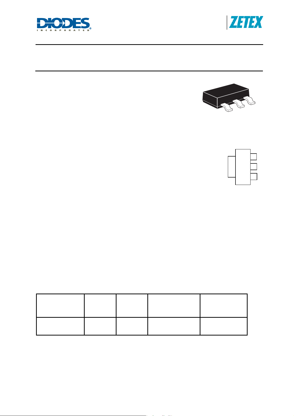
SOT223 Package
S
QUANTITY PER
REEL
1,000 units
S
D
IN
ZXMS6005SG
Document Number DS32249 Rev. 1 - 2
1 of 9
www.diodes.com
June 2010
© Diodes Incorporated

A
f
o
Product Line o
Diodes Incorporated
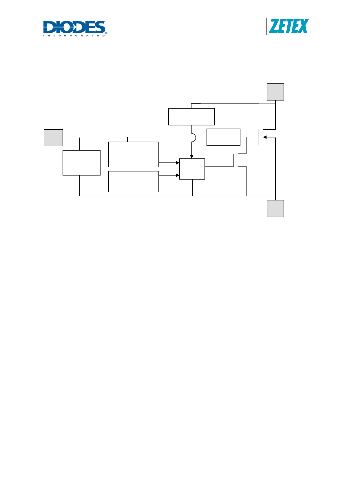
FUNCTIONAL BLOCK DIAGRAM
IN
Human
body ESD
protection
Over temperature
protection
Over current
protection
Over Voltage
Protection
Logic
dV/dt
limitati
n
D
S
APPLICATIONS AND INFORMATION
• Especially suited for loads with a high in-rush current such as lamps and motors.
• All types of resistive, inductive and capacitive loads in switching applications.
• μC compatible power switch for 12V DC applications.
• Automotive rated.
• Replaces electromechanical relays and discrete circuits.
• Linear Mode capability - the current-limiting protection circuitry is designed to de-activate
at low V
therefore determined by the thermal capability of the package/board combination, rather
than by the protection circuitry. This does not compromise the product’s ability to selfprotect at low V
to minimise on state power dissipation. The maximum DC operating current is
DS
.
DS
ZXMS6005SG
Document Number DS32249 Rev. 1 - 2
2 of 9
www.diodes.com
June 2010
© Diodes Incorporated

A
f
)
Product Line o
Diodes Incorporated
ABSOLUTE MAXIMUM RATINGS
PARAMETER SYMBOL LIMIT UNIT
Continuous Drain-Source Voltage VDS 60 V
Drain-Source Voltage for short circuit protection V
24 V
DS(SC
Continuous Input Voltage VIN -0.5 ... +6 V
Continuous Input Current
-0.2V≤V
V
IN
≤6V
IN
<-0.2V or VIN>6V
Operating Temperature Range Tj, -40 to +150
Storage Temperature Range T
Power Dissipation at TA =25°C (a)
Linear Derating Factor
Power Dissipation at TA =25°C (b)
Linear Derating Factor
I
IN
No limit
│I
│≤2
IN
-55 to +150
stg
P
1.0
D
8.0
P
1.6
D
12.8
mW/°C
mW/°C
mA
°C
°C
W
W
Pulsed Drain Current @ VIN=3.3V IDM 5 A
Pulsed Drain Current @ VIN=5V IDM 6 A
Continuous Source Current (Body Diode) (a) IS 2.5 A
Pulsed Source Current (Body Diode) ISM 10 A
480 mJ
Unclamped single pulse inductive energy, Tj=25°C,
=0.5A, VDD=24V
I
D
E
AS
Electrostatic Discharge (Human Body Model) V
Charged Device Model V
4000 V
ESD
1000 V
CDM
THERMAL RESISTANCE
PARAMETER SYMBOL VALUE UNIT
Junction to Ambient (a) R
Junction to Ambient (b) R
Junction to Case (c) R
125
θJA
83
θJA
39
θJC
°C/W
°C/W
°C/W
NOTES
(a) For a device surface mounted on 15mm x 15mm single sided 1oz weight copper on 1.6mm FR4 board, in
still air conditions. Sink split drain 80% and source 20% to isolate connections.
(b) For a device surface mounted on 50mm x 50mm single sided 2oz weight copper on 1.6mm FR4 board, in
still air conditions. Sink split drain 80% and source 20% to isolate connections.
(c) Thermal resistance between junction and the mounting surfaces of drain and source pins.
ZXMS6005SG
Document Number DS32249 Rev. 1 - 2
3 of 9
www.diodes.com
June 2010
© Diodes Incorporated
 Loading...