Diodes ZXMS6005DT8 User Manual

A
f
Product Line o
Green
Diodes Incorporated
ZXMS6005DT8
Product Summary
Continuos drain source voltage 60V
On-state resistance 200m
Nominal load current (V
Clamping Energy 210mJ
= 5V) 1.8A
IN
Description
The ZXMS6005DT8 is a dual self protected low side MOSFET with
logic level input. It integrates over-temperature, over-current, over-
voltage (active clamp) and ESD protected logic level functionality. The
ZXMS6005DT8 is ideal as a general purpose switch driven from 3.3V
or 5V microcontrollers in harsh environments where standard
MOSFETs are not rugged enough.
ADVANCE INFORMATION
Applications
Lamp Driver
Motor Driver
Relay Driver
Solenoid Driver
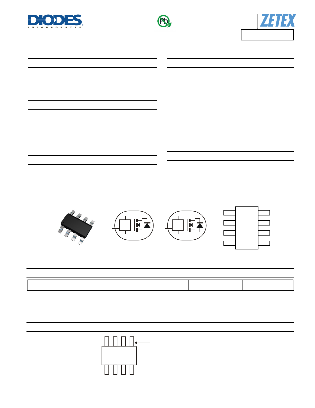
SM-8
IN1
Top View
60V DUAL N-CHANNEL SELF PROTECTED ENHANCEMENT MODE
INTELLIFET® MOSFET
Features and Benefits
Compact Dual Package
Low Input Current
Logic Level Input (3.3V and 5V)
Short Circuit Protection with Auto Restart
Over Voltage Protection (active clamp)
Thermal Shutdown with Auto Restart
Over-Current Protection
Input Protection (ESD)
High Continuous Current Rating
Lead-Free Finish; RoHS compliant (Note 1 & 2)
Halogen and Antimony Free. “Green” Device (Note 3)
Qualified to AEC-Q101 Standards for High Reliability
Mechanical Data
Case: SM-8
Case Material: Molded Plastic, “Green” Molding Compound.
UL Flammability Classification Rating 94V-0
Moisture Sensitivity: Level 1 per J-STD-020
Terminals: Matte Tin Finish
Weight: 0.117 grams (approximate)
D1
IN2
S1
Device Symbol
D2
S2
IN1
S1
IN2
S2
1
D1
D1
D2
D2
Top view
Pin-Out
Ordering Information (Note 4)
Product Marking Reel size (inches) Tape width (mm) Quantity per reel
ZXMS6005DT8TA ZXMS6005D 7 12 1,000
Notes: 1. No purposely added lead. Fully EU Directive 2002/95/EC (RoHS) & 2011/65/EU (RoHS 2) compliant.
2. See http://www.diodes.com/quality/lead_free.html for more information about Diodes Incorporated’s definitions of Halogen- and Antimony-free, "Green"
and Lead-free.
3. Halogen- and Antimony-free "Green” products are defined as those which contain <900ppm bromine, <900ppm chlorine (<1500ppm total Br + Cl) and
<1000ppm antimony compounds.
4. For packaging details, go to our website at http”//www.diodes.com/products/packages.html.
Marking Information
IntelliFET® is a trademark of Diodes Incorporated, registered in the United States and other jurisdictions worldwide.
ZXMS
6005D
Top View
ZXMS6005DT8
Document number: DS32248 Rev. 2 - 2
Pin 1
ZXMS6005D = Product Type Marking Code
1 of 9
www.diodes.com
March 2013
© Diodes Incorporated

A
f
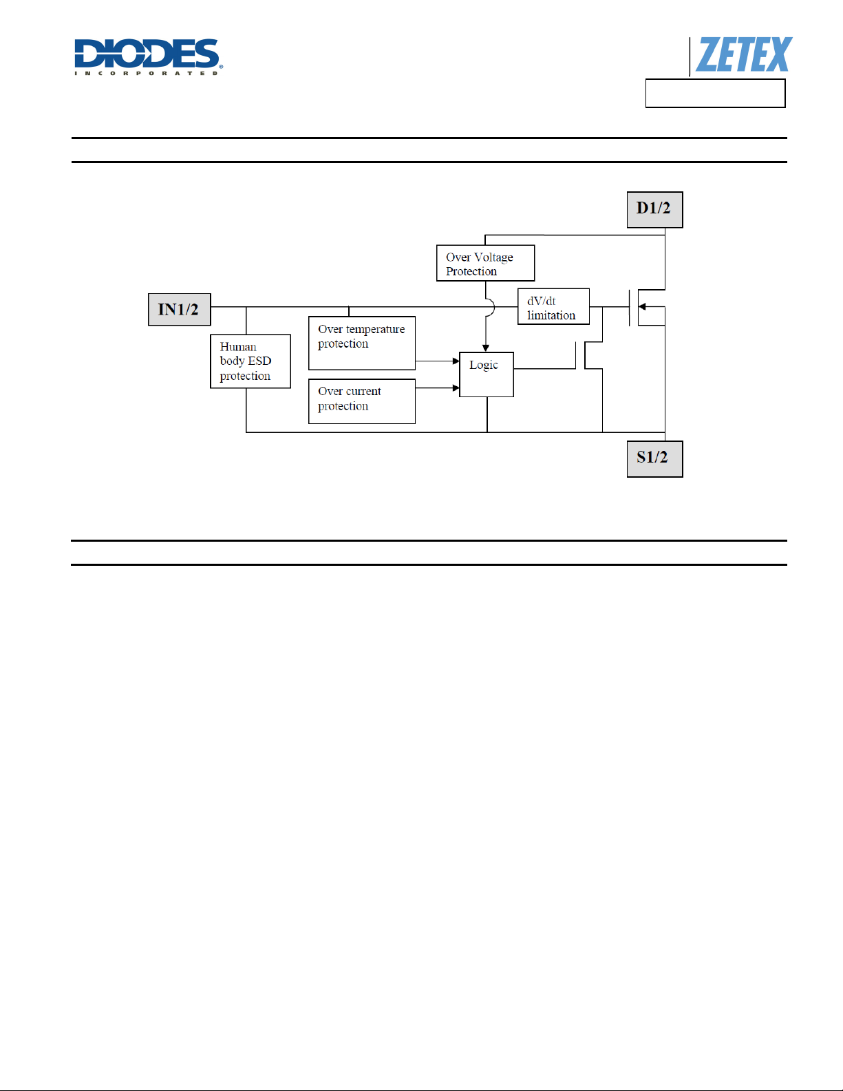
Functional Block Diagram
ADVANCE INFORMATION
Product Line o
Diodes Incorporated
ZXMS6005DT8
Application Information
Two completely isolated independent channels
Especially suited for loads with a high in-rush current such as lamps and motors.
All types of resistive, inductive and capacitive loads in switching applications.
μC compatible power switch for 12V DC applications.
Automotive rated.
Replaces electromechanical relays and discrete circuits.
Linear Mode capability - the current-limiting protection circuitry is designed to de-activate at low V
The maximum DC operating current is therefore determined by the thermal capability of the package/board combination, rather than by the
protection circuitry. This does not compromise the product’s ability to self-protect at low V
IntelliFET® is a trademark of Diodes Incorporated, registered in the United States and other jurisdictions worldwide.
ZXMS6005DT8
Document number: DS32248 Rev. 2 - 2
2 of 9
www.diodes.com
DS
to minimise on state power dissipation.
DS
.
March 2013
© Diodes Incorporated

A
f
)
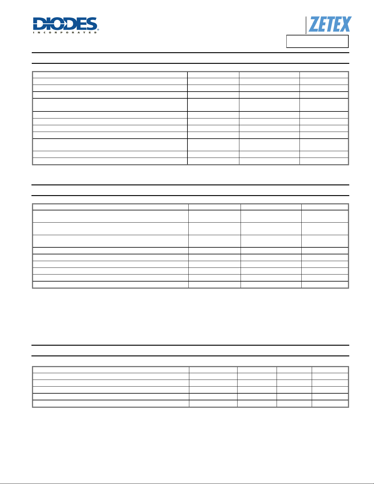
Maximum Ratings (@T
= +25°C, unless otherwise specified.)
A
Characteristic Symbol Value Units
Continuous Drain-Source Voltage
Drain-Source Voltage For Short Circuit Protection
Continuous Input Voltage
Continuous Input Current @ -0.2V ≤ VIN ≤ 6V
Continuous Input Current @V
< -0.2V or VIN > 6V
IN
V
DS(SC
V
DS
V
IN
I
IN
Pulsed Drain Current @VIN = 3.3V ( Note 7) IDM
Pulsed Drain Current @VIN = 5V ( Note 7) IDM
Continuous Source Current (Body Diode) (Note 5)
Pulsed Source Current (Body Diode)
Unclamped Single Pulse Inductive Energy,
= +25C, ID = 0.5A, VDD = 24V
T
J
Electrostatic Discharge (Human Body Model)
Charged Device Model
V
V
I
E
ESD
CDM
I
SM
S
AS
ADVANCE INFORMATION
Thermal Characteristics (@T
= +25°C, unless otherwise specified.)
A
Characteristic Symbol Value Units
Power Dissipation at TA = +25C (Notes 5 & 8)
Linear Derating Factor
Power Dissipation at TA = +25C (Notes 5 & 9)
Linear Derating Factor
Power Dissipation at TA = +25C (Notes 6 & 8)
Linear Derating Factor
Thermal Resistance, Junction to Ambient (Notes 5 & 8)
Thermal Resistance, Junction to Ambient (Notes 5 & 9)
Thermal Resistance, Junction to Case (Notes 6 & 8)
Thermal Resistance, Junction to Case (Note 10)
Operating Temperature Range
Storage Temperature Range
Notes: 5. For a dual device surface mounted on a 25mm x 25mm single sided 1oz weight copper split down the middle on 1.6mm FR4 board, in still air conditions.
6. For a dual device surface mounted on FR4 PCB measured at t≤ 10sec
7. Repetitive rating25mm x 25mm FR4 PCB, D = 0.02, Pulse width = 300µs – pulse width limited by junction temperature. Refer to transient thermal
impedance graph.
8. For a dual device with one active die.
9. For a dual device with 2 active die running at equal power.
10. Thermal resistance from junction to the mounting surface of the drain pin.
P
D
P
D
P
D
R
θJA
R
θJA
R
θJC
R
θJC
T
J
T
STG
Diodes Incorporated
ZXMS6005DT8
60 V
24 V
-0.5 ... +6 V
No limit
│≤2
│I
IN
5 A
6 A
2.5 A
10 A
210 mJ
4000 V
1000 V
1.16
9.28
1.67
13.3
2.13
17
108
75
58.7
26.5
-40 to +150
-55 to +150
Product Line o
mA
W
mW/C
W
mW/C
W
mW/C
C/W
C/W
C/W
C/W
C
C
Recommended Operating Conditions
The ZXMS6005DT8 is optimized for use with µC operating from 3.3V and 5V supplies.
Characteristic Symbol Min Max Unit
Input Voltage Range
Ambient Temperature Range
High Level Input Voltage for MOSFET to be on
Low Level Input Voltage for MOSFET to be off
Peripheral Supply Voltage (voltage to which load is referred)
V
IN
T
A
V
IH
V
IL
V
P
IntelliFET® is a trademark of Diodes Incorporated, registered in the United States and other jurisdictions worldwide.
ZXMS6005DT8
Document number: DS32248 Rev. 2 - 2
3 of 9
www.diodes.com
0 5.5 V
-40 125 °C
3 5.5 V
0 0.7 V
0 24 V
March 2013
© Diodes Incorporated
 Loading...