

Page 1
A
f
Product Line o
Diodes Incorporated
ZXMS6004DT8
60V N-CHANNEL SELF PROTECTED ENHANCEMENT MODE
™
INTELLIFET
MOSFET
SUMMARY
Continuous drain source voltage 60 V
On-state resistance 500 mΩ
Nominal load current (V
Clamping Energy 210 mJ
DESCRIPTION
The ZXMS6004DT8 is a dual self protected low side MOSFET
with logic level input. It integrates over-temperature, overcurrent, over-voltage (active clamp) and ESD protected logic level
functionality independently per channel. The ZXMS6004DT8 is
ideal as a general purpose switch driven from 3.3V or 5V
microcontrollers in harsh environments where standard
MOSFETs are not rugged enough.
FEATURES
• Compact dual package
• Low input current
• Logic Level Input (3.3V and 5V)
• Short circuit protection with auto restart
• Over voltage protection (active clamp)
• Thermal shutdown with auto restart
• Over-current protection
• Input Protection (ESD)
• High continuous current rating
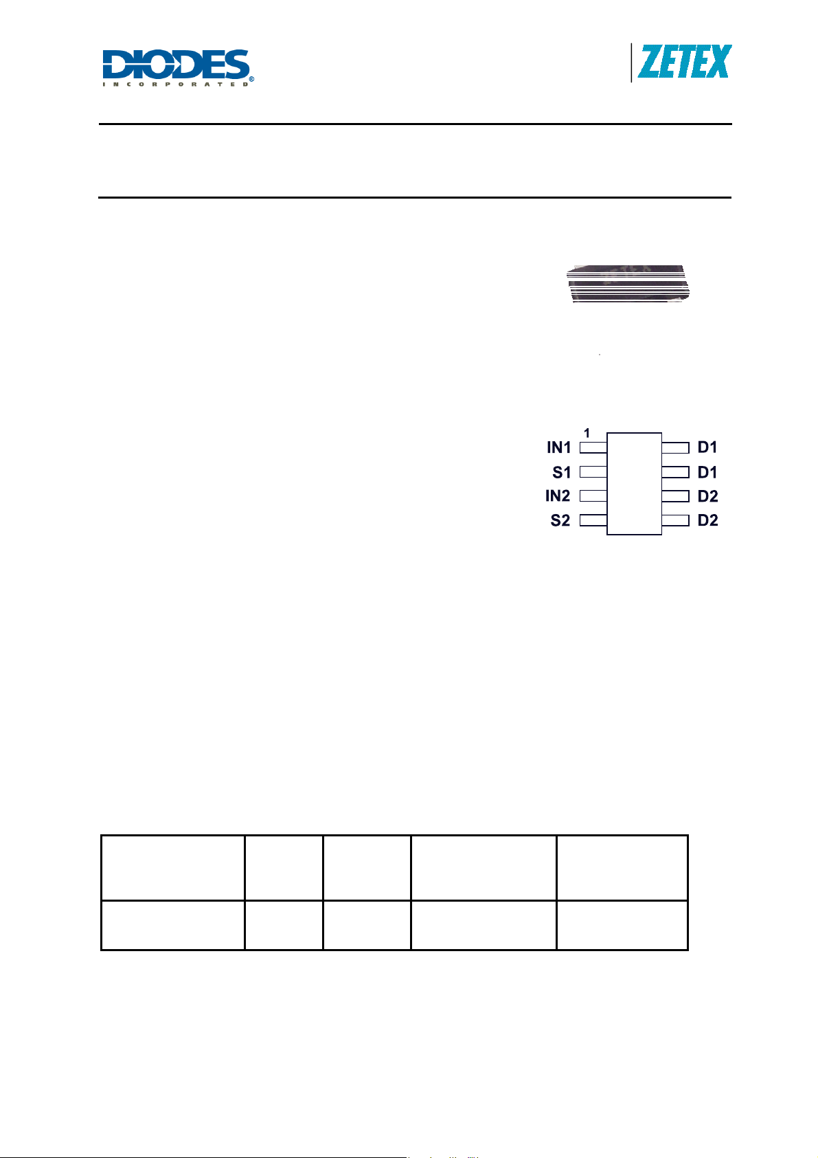
ORDERING INFORMATION
DEVICE
ZXMS6004DT8TA
= 5V) 1.2 A
IN
PART
MARK
ZXMS
6004D
REEL SIZE
(inches)
7
TAPE WIDTH
(mm)
12 embossed
SM8 Package
QUANTITY PER
REEL
1,000 units
ZXMS6004DT8
Document Number DS32245 Rev. 1 - 2
1 of 9
www.diodes.com
June 2010
© Diodes Incorporated
Page 2
A
f
otectio
o
Product Line o
Diodes Incorporated
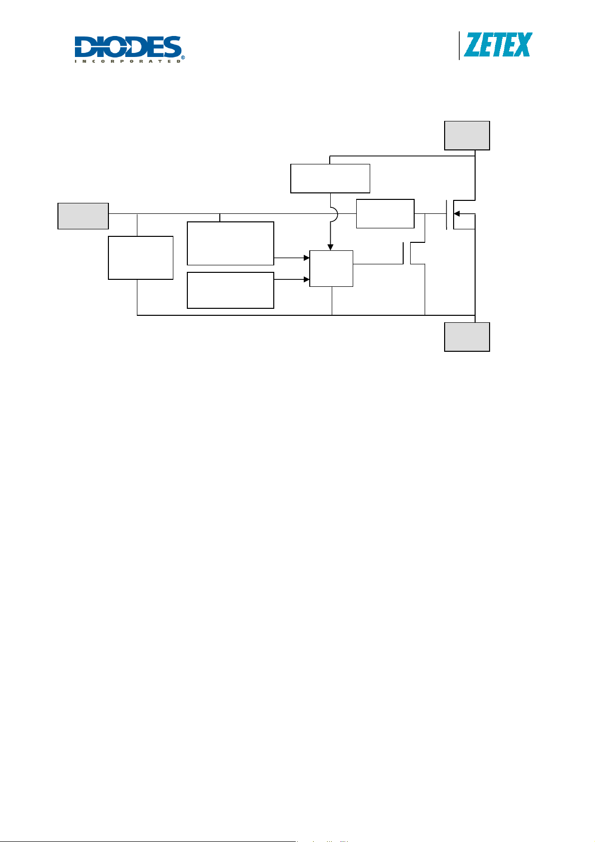
FUNCTIONAL BLOCK DIAGRAM
IN1/2
Human
body ESD
protection
Over temperature
protection
Over current
protection
Over Voltage
Pr
n
Logic
dV/dt
limitati
n
D1/2
S1/2
APPLICATIONS AND INFORMATION
• Two completely isolated independent channels
• Especially suited for loads with a high in-rush current such as lamps and motors.
• All types of resistive, inductive and capacitive loads in switching applications.
• μC compatible power switch for 12V and 24V DC applications.
• Automotive rated.
• Replaces electromechanical relays and discrete circuits.
• Linear Mode capability - the current-limiting protection circuitry is designed to de-activate
at low V
therefore determined by the thermal capability of the package/board combination, rather
than by the protection circuitry. This does not compromise the product’s ability to selfprotect at low V
to minimise on state power dissipation. The maximum DC operating current is
DS
.
DS
ZXMS6004DT8
Document Number DS32245 Rev. 1 - 2
2 of 9
www.diodes.com
June 2010
© Diodes Incorporated
Page 3
A
f
)
Product Line o
Diodes Incorporated
ABSOLUTE MAXIMUM RATINGS
PARAMETER SYMBOL LIMIT UNIT
Continuous Drain-Source Voltage VDS 60 V
Drain-Source Voltage for short circuit protection V
36 V
DS(SC
Continuous Input Voltage VIN -0.5 ... +6 V
Continuous Input Current
-0.2V≤V
V
IN
≤6V
IN
<-0.2V or VIN>6V
Operating Temperature Range Tj, -40 to +150
Storage Temperature Range T
Power Dissipation at TA =25°C (a)(d)
Linear Derating Factor
Power Dissipation at TA =25°C (a)(e)
Linear Derating Factor
Power Dissipation at TA =25°C (b)(d)
Linear Derating Factor
I
IN
No limit
│I
│≤2
IN
-55 to +150
stg
P
1.16
D
9.28
P
1.67
D
13.3
P
2.13
D
17
mW/°C
mW/°C
mW/°C
mA
°C
°C
W
W
W
Pulsed Drain Current @ VIN=3.3V (c) IDM 2 A
Pulsed Drain Current @ VIN=5V (c) IDM 2.5 A
Continuous Source Current (Body Diode) (a) IS 1 A
Pulsed Source Current (Body Diode) (c) ISM 5 A
E
Unclamped single pulse inductive energy, Tj=25°C,
=0.5A, VDD=24V
I
D
Electrostatic Discharge (Human Body Model) V
Charged Device Model V
210 mJ
AS
4000 V
ESD
1000 V
CDM
THERMAL RESISTANCE
PARAMETER SYMBOL VALUE UNIT
Junction to Ambient (a)(d) R
Junction to Ambient (a)(e) R
Junction to Ambient (b)(d) R
Junction to Case (f) R
108
θJA
75
θJA
58.7
θJA
26.5
θJC
°C/W
°C/W
°C/W
°C/W
NOTES
(a) For a dual device surface mounted on a 25mm x 25mm FR4 PCB single sided 1oz weight copper split
down the middle on 1.6mm FR4 board, in still air conditions.
(b) For a dual device surface mounted on FR4 PCB measured at t ≤ 10sec
(c) Repetitive rating 25mm x 25mm FR4 PCB, D=0.02 pulse width=300µs – pulse width limited by junction
temperature. Refer to transient Thermal Impedance Graph.
(d) For a dual device with one active die.
(e) For dual device with 2 active die running at equal power.
(f) Thermal resistance from junction to solder-point (at the end of the drain lead)
ZXMS6004DT8
Document Number DS32245 Rev. 1 - 2
3 of 9
www.diodes.com
June 2010
© Diodes Incorporated
Page 4

A
f
Product Line o
Diodes Incorporated
RECOMMENDED OPERATING CONDITIONS
The ZXMS6004DT8 is optimised for use with µC operating from 3.3V and 5V supplies.
Symbol Description Min Max Units
VIN Input voltage range 0 5.5 V
TA Ambient temperature range -40 125 °C
VIH High level input voltage for MOSFET to be on 3 5.5 V
VIL Low level input voltage for MOSFET to be off 0 0.7 V
VP Peripheral supply voltage (voltage to which load is referred) 0 36 V
CHARACTERISTICS
Limited by Over-Current Protection
DS(on)
DC
1s
100ms
10ms
=25°C
amb
110
1ms
Limit of s/c protection
100m
Drain Current (A)
D
10m
I
Limited
by R
1
Single Pulse
T
See Note (a)(d)
VDS Drain-Source Voltage (V)
Safe Operating Area
120
T
=25°C
amb
See Note (a )(d )
100
80
D=0.5
60
40
D=0.2
20
0
100µ 1m 10m 100m 1 10 100 1k
Thermal Resistance (°C/W)
Single Pulse
D=0.05
D=0.1
Pulse Width (s)
Transient Thermal Impedance
1.6
1.4
1.2
1.0
0.8
0.6
0.4
0.2
0.0
0 25 50 75 100 125 150
Max Power Dissipation (W)
1 active die
2 active die
Temperature (°C)
Derating Curve
Single Pulse
100
10
Maximum Power (W)
1
100µ 1m 10m 100m 1 10 100 1k
T
amb
See Note (a)(d)
Pulse Width (s)
Pulse Power Dissipation
=25°C
ZXMS6004DT8
Document Number DS32245 Rev. 1 - 2
4 of 9
www.diodes.com
June 2010
© Diodes Incorporated
Page 5

A
f
)
)
)
Product Line o
Diodes Incorporated
ELECTRICAL CHARACTERISTICS (at T
= 25°C unless otherwise stated).
amb
PARAMETER SYMBOL MIN TYP MAX UNIT CONDITIONS
Static Characteristics
Drain-Source Clamp Voltage V
Off state Drain Current I
Off state Drain Current I
Input Threshold Voltage V
Input Current IIN 60 100
Input Current IIN 120 200
Input Current while over
60 65 70 V ID=10mA
DS(AZ)
500 nA VDS=12V, VIN=0V
DSS
1 uA VDS=36V, VIN=0V
DSS
0.7 1 1.5 V VDS=VGS, ID=1mA
IN(th
VIN=+3V
VIN=+5V
VIN=+5V
220
μA
μA
μA
temperature active
Static Drain-Source On-State
Resistance
Static Drain-Source On-State
Resistance
Continuous Drain Current (a)(e) ID 0.9 A
R
400 600
DS(on)
R
350 500
DS(on)
mΩ
mΩ
VIN=+3V, ID=0.5A
VIN=+5V, ID=0.5A
=3V; TA=25°C
V
IN
Continuous Drain Current (a)(e) ID 1.0 A
Continuous Drain Current (a)(d) ID 1.1 A
Continuous Drain Current (a)(d) ID 1.2 A
Current Limit (g) I
Current Limit (g) I
Dynamic Characteristics
Turn On Delay Time t
Rise time tr 10
0.7 1.7 A VIN=+3V,
D(LIM
1 2.2 A VIN=+5V
D(LIM
5
d(on)
μs
μs
=5V; TA=25°C
V
IN
=3V; TA=25°C
V
IN
=5V; TA=25°C
V
IN
VDD=12V, ID=0.5A,
=5V
V
GS
Turn Off Delay Time t
Fall Time ff 15
45
d(off)
μs
μs
Notes:
(g) The drain current is restricted only when the device is in saturation (see graph ‘typical output
characteristic’). This allows the device to be used in the fully on state without interference from
the current limit. The device is fully protected at all drain currents, as the low power dissipation
generated outside saturation makes current limit unnecessary.
ZXMS6004DT8
Document Number DS32245 Rev. 1 - 2
5 of 9
www.diodes.com
June 2010
© Diodes Incorporated
Page 6

A
f
Product Line o
Diodes Incorporated
PARAMETER SYMBOL MIN TYP MAX UNIT CONDITIONS
Over-temperature Protection
Thermal Overload Trip
TJT 150 175
°C
Temperature (h)
Thermal hysteresis (h) 10
°C
Note:
(h) Over-temperature protection is designed to prevent device destruction under fault conditions.
Fault conditions are considered as “outside” normal operating range, so this part is not designed
to withstand over-temperature for extended periods..
ZXMS6004DT8
Document Number DS32245 Rev. 1 - 2
6 of 9
www.diodes.com
June 2010
© Diodes Incorporated
Page 7

A
f
Product Line o
Diodes Incorporated
TYPICAL CHARACTERISTICS
3
2
1
Drain Current (A)
D
I
0
0123456789101112
TA = 25°C
VDS Drain-Source Vol tage (V)
Typical Output C haracteristic
1.4
1.2
1.0
0.8
0.6
0.4
On-Resistance (Ω)
0.2
DS(on)
R
0.0
1.5 2.0 2.5 3.0 3.5 4.0 4.5 5.0
VIN Input Voltage (V)
ID = 0.5A
TJ = 150°C
TJ = 25°C
On-Resistance vs Input Voltage
0.9
0.8
0.7
0.6
0.5
0.4
On-Resistance (Ω)
0.3
DS(on)
R
0.2
-75 -50 -25 0 25 50 75 100 125 150
VIN = 3V
TJ Junction Te mperatu re (°C)
On-Resistance vs Temperature
VIN = 5V
V
IN
5.5V
5.0V
4.5V
4.0V
3.5V
3.0V
2.5V
2.0V
120
100
80
60
40
20
Input Current (μA)
IN
I
0
012345
VIN Input Voltage (V)
Input Current v s Inpu t V oltag e
1.4
1.3
1.2
1.1
1.0
0.9
Threshold Voltage (V)
TH
0.8
V
-75 -50 -25 0 25 50 75 100 125 150
VIN = V
ID = 1mA
TJ Junction T e mperature (°C)
Threshold Voltage vs Tem perature
10
TJ=150°C
1
0.1
Source Curent (A)
S
I
0.01
0.4 0.6 0.8 1.0 1.2
TJ=25°C
VSD Source-Drain Voltage (V)
Reverse Diode Characteristic
DS
ZXMS6004DT8
Document Number DS32245 Rev. 1 - 2
7 of 9
www.diodes.com
June 2010
© Diodes Incorporated
Page 8

A
f
Product Line o
Diodes Incorporated
12
10
8
6
4
2
Drain-Source Voltage (V)
0
-50 0 50 100 150 200 250 300
V
DS
ID=500mA
V
IN
Time (μs)
Switching Speed
4.0
3.5
3.0
2.5
2.0
1.5
1.0
Drain Current (A )
D
0.5
I
0.0
02040
VIN = 5V
VDS = 15V
RD = 0Ω
Time (ms)
Typical Short Circuit Protection
12
V
10
8
6
4
2
Drain-Source Voltage (V)
0
-50 0 50 100 150 200 250 300
DS
V
IN
ID=500mA
Time (μs)
Switching Speed
ZXMS6004DT8
Document Number DS32245 Rev. 1 - 2
8 of 9
www.diodes.com
June 2010
© Diodes Incorporated
Page 9

A
f
Product Line o
Diodes Incorporated
DIODES INCORPORATED MAKES NO WARRANTY OF ANY KIND, EXPRESS OR IMPLIED, WITH REGARDING TO THIS
DOCUMENT, INCLUDING, BUT NOT LIMITED TO, THE IMPLIED WARRANTIES OF MERCHANTABILITY AND FITNESS
FOR A PARTICULAR PURPOSE (AND THEIR EQUIVALENTS UNDER THE LAWS OF ANY JURISDICTION).
Diodes Incorporated and its subsidiaries reserve the right to make modifications, enhancements, improvements, corrections or
other changes without further notice to this document and any product described herein. Diodes Incorporated does not assume
any liability arising out of the application or use of this document or any product described herein; neither does Diodes
Incorporated convey any license under its patent or trademark rights, nor the rights of others. Any Customer or user of this
document or products described herein in such applications shall assume all risks of such use and will agree to hold Diodes
Incorporated and all the companies whose products are represented on Diodes Incorporated website, harmless against all
damages.
Diodes Incorporated does not warrant or accept any liability whatsoever in respect of any products purchased through
unauthorized sales channel.
Should Customers purchase or use Diodes Incorporated products for any unintended or unauthorized application, Customers
shall indemnify and hold Diodes Incorporated and its representatives harmless against all claims, damages, expenses, and
attorney fees arising out of, directly or indirectly, any claim of personal injury or death associated with such unintended or
unauthorized application.
Products described herein may be covered by one or more United States, international or foreign patents pending. Product
names and markings noted herein may also be covered by one or more United States, international or foreign trademarks.
Diodes Incorporated products are specifically not authorized for use as critical components in life support devices or systems
without the express written approval of the Chief Executive Officer of Diodes Incorporated. As used herein:
A. Life support devices or systems are devices or systems which:
1. are intended to implant into the body, or
2. support or sustain life and whose failure to perform when properly used in accordance with instructions for use
provided in the labeling can be reasonably expected to result in significant injury to the user.
B. A critical component is any component in a life support device or system whose failure to perform can be reasonably
expected to cause the failure of the life support device or to affect its safety or effectiveness.
Customers represent that they have all necessary expertise in the safety and regulatory ramifications of their life support
devices or systems, and acknowledge and agree that they are solely responsible for all legal, regulatory and safety-related
requirements concerning their products and any use of Diodes Incorporated products in such safety-critical, life support devices
or systems, notwithstanding any devices- or systems-related information or support that may be provided by Diodes
Incorporated. Further, Customers must fully indemnify Diodes Incorporated and its representatives against any damages
arising out of the use of Diodes Incorporated products in such safety-critical, life support devices or systems.
Copyright © 2010, Diodes Incorporated
www.diodes.com
IMPORTANT NOTICE
LIFE SUPPORT
ZXMS6004DT8
Document Number DS32245 Rev. 1 - 2
9 of 9
www.diodes.com
June 2010
© Diodes Incorporated
 Loading...