

Page 1
ZXMS6001N3
60V N-channel self protected enhancement mode
INTELLIFETTM MOSFET
Summary
Continuous drain source voltage VDS = 60V
On-state resistance 675mΩ
Max nominal load current (a) 1.1A (V
Min nominal load current (c) 0.7A (V
Clamping Energy 550mJ
= 5V)
IN
= 5V)
IN
Description
Low input current self protected low side MOSFET intended for Vin=5V
applications. Monolithic over temperature, over current, over voltage
(active clamp) and ESD protected logic level functionality. Intended as
a general purpose switch.
Note:
The tab is connected to the source pin and must be electrically isolated
from the drain pin. Connection of significant copper to the drain pin is
recommended for best thermal performance.
Features
• Short circuit protection with auto restart
• Over voltage protection (active clamp)
• Thermal shutdown with auto restart
• Over-current protection
• Input protection (ESD)
• Load dump protection (actively protects load)
• Low input current
S
S
D
IN
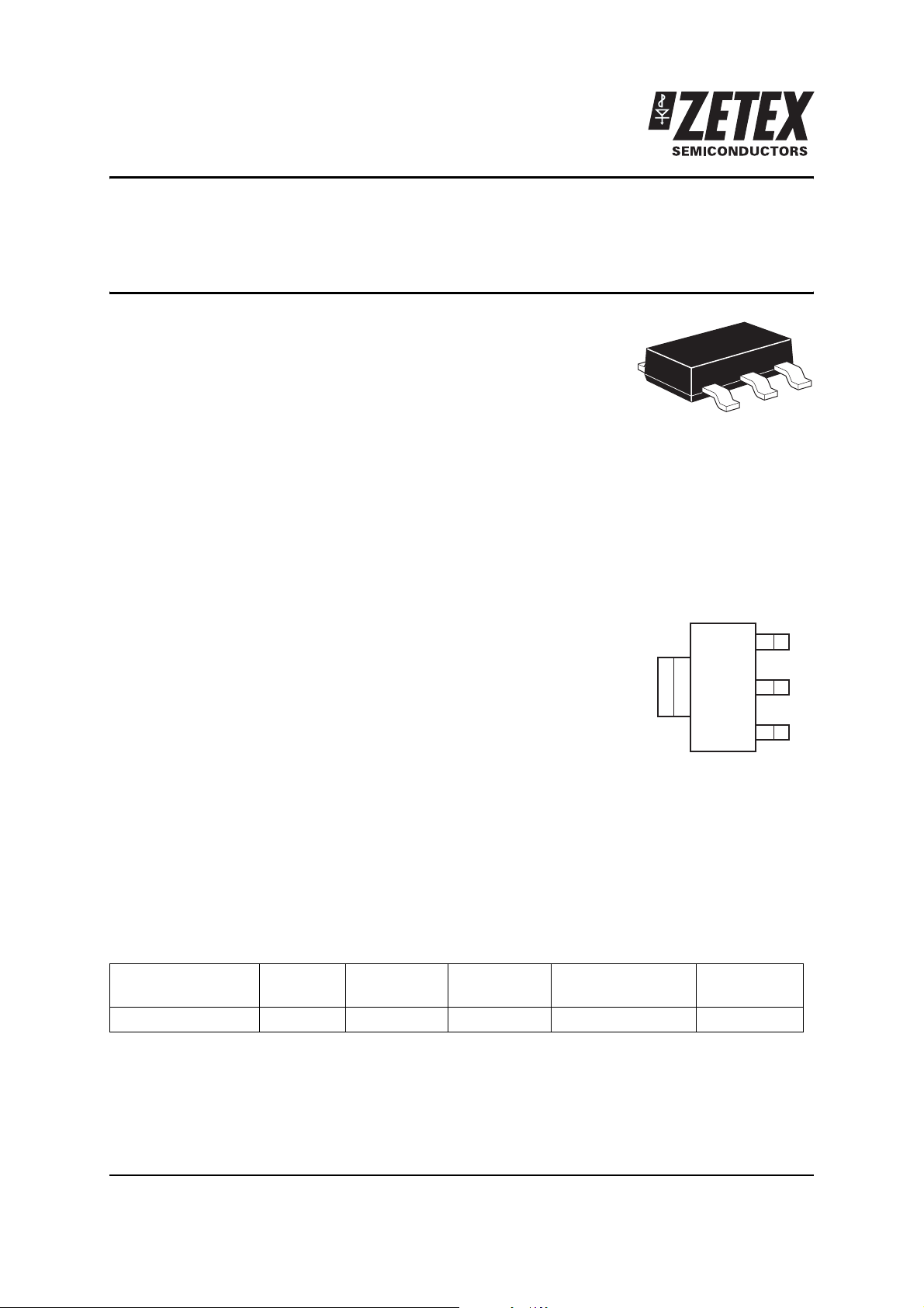
SOT223
Ordering information
Device Package Part mark Reel size
(inches)
ZXMS6001N3TA SOT223 ZXMS6001 7 12 embossed 1,000
Issue 1 - January 2008 1 www.zetex.com
© Zetex Semiconductors plc 2008
Tape width
(mm)
Quantity
per reel
Page 2
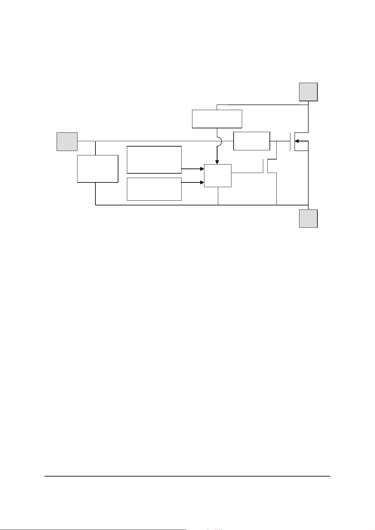
Functional block diagram
ZXMS6001N3
Over Voltage
Protection
IN
Human body
ESD
protection
Over current
protection
Logic
Over temperature
protection
dV/dt
limitation
Applications and information
• Especially suited for loads with a high in-rush current such as lamps and motors.
• All types of resistive, inductive and capacitive loads in switching applications.
D
S
• µC compatible power switch for 12V and 24V DC applications.
• Automotive rated.
• Replaces electromechanical relays and discrete circuits.
Linear Mode capability - the current-limiting protection circuitry is designed to de-activate at low
Vds, in order not to compromise the load current during normal operation. The design max DC
operating current is therefore determined by the thermal capability of the package/board
combination, rather than by the protection circuitry. This does not compromise the products
ability to self protect itself at low V
DS
.
Issue 1 - January 2008 2 www.zetex.com
© Zetex Semiconductors plc 2008
Page 3
ZXMS6001N3
Absolute maximum ratings
Parameter Symbol Limit Unit
Continuous Drain-Source Voltage V
Drain-Source Voltage for short circuit protection V
= 5V V
IN
Continuous Input Voltage V
Peak Input Voltage V
Continuous Input Current
DS
DS(SC)
IN
IN
I
IN
-0.2V=VIN=10V
V
<-0.2V or VIN>10V
IN
Operating Temperature Range T
Storage Temperature Range T
Power Dissipation at T
Power Dissipation at T
=25°C
A
=25°C
A
Continuous Drain Current @ V
Continuous Drain Current @ V
Continuous Source Current (Body Diode)
Pulsed Source Current (Body Diode)
(a)
(c)
=5V; TA=25°C
IN
=5V; TA=25°C
IN
(b)
(a)
(c)
(a)
Unclamped single pulse inductive energy E
Load dump protection V
Electrostatic Discharge (Human Body Model) V
,
j
stg
P
D
P
D
I
D
I
D
I
S
I
S
AS
LoadDump
ESD
DIN humidity category, DIN 40 040 E
IEC climatic category, DIN IEC 68-1 40/150/56
60 V
36 V
-0.2 ... +10 V
-0.2 ... +20 V
mA
No limit
| I
| ≤2
IN
-40 to +150
-55 to +150
1.5 W
0.6 W
1.1 A
0.7 A
2.0 A
3.3 A
550 mJ
80 V
4000 V
°C
°C
Thermal resistance
Parameter Symbol Value Unit
Junction to ambient
Junction to ambient
Junction to ambient
NOTES:
(a) For a device surface mounted on 25mm x 25mm x 1.6mm FR4 board with a high coverage of single sided 2oz weight
copper. Allocation of 6cm
isolated.
(b) For a device surface mounted on FR4 board as (a) and measured at t<=10s.
(c) For a device surface mounted on FR4 board with the minimum copper required for electrical connections.
(a)
(b)
(c)
2
copper 33% to source tab and 66% to drain pin with source tab and drain pin electrically
Issue 1 - January 2008 3 www.zetex.com
© Zetex Semiconductors plc 2008
R
R
R
⍜JA
⍜JA
⍜JA
83 °C/W
45 °C/W
208 °C/W
Page 4

ZXMS6001N3
Recommended operating conditions
The ZXMS6001 is optimized for use with µC operating from 5V supplies.
Symbol Description Min Max Units
V
T
V
V
Input voltage range 0 6 V
IN
Ambient temperature range -40 125 °C
A
High level input voltage for MOSFET
IH
Peripheral supply voltage
P
(d)
46V
(voltage to which load is referred)
60 V
Electrical characteristics (at T
= 25°C unless otherwise stated).
amb
Parameter Symbol Min Typ Max Unit Conditions
Static Characteristics
Drain-Source Clamp
V
DS(AZ)
60 70 75 V ID=10mA
Voltage
Off state Drain Current I
Off state Drain Current I
Input Threshold Voltage
(d)
Input Current I
Input Current I
DSS
DSS
V
IN
IN
IN(th)
11.82.5VVDS=VGS, ID=10mA
0.1 3 AVDS=12V, VIN=0V
315AVDS=32V, VIN=0V
150 AVIN=+3V
335 500 AVIN=+5V, all
circumstances
Static Drain-Source
R
DS(on)
12Ω VIN=3V, ID=0.1A
On-State Resistance
Static Drain-Source
R
DS(on)
520 675 mΩ VIN=5V, ID=0.7A
On-State Resistance
Current Limit
(e)
I
D(LIM)
11.83 AVIN=5V, VDS>5V
Dynamic Characteristics
Tur n -On Tim e
(V
to 90% ID)
IN
Turn-Off time
to 90% ID)
(V
IN
Slew Rate On
(70 to 50% V
DD
Slew Rate Off
(50 to 70% V
DD
)
)
t
on
t
off
-dVDS/dt
DV
/dt
DS
on
on
27 40 sRL=22Ω, VIN=0 to 5V,
=12V
V
DD
26 40 sRL=22Ω, VIN=5V to 0V,
=12V
V
DD
1.4 10 V/sRL=22Ω, VIN=0 to 5V,
=12V
V
DD
1.2 10 V/sRL=22Ω, VIN=5V to 0V,
V
=12V
DD
NOTES:
(d) Recommended input voltage range over which protection circuits function as specified.
(e) The drain current is limited to a reduced value when Vds exceeds a safe level
Issue 1 - January 2008 4 www.zetex.com
© Zetex Semiconductors plc 2008
Page 5

ZXMS6001N3
Parameter Symbol Min Typ Max Unit Conditions
Protection Functions (f)
Minimum input voltage
for over temperature
protection
Maximum input voltage
for over temperature
protection
Thermal Overload Trip
Temperature
Thermal hysteresis 8 °C
Unclamped single pulse
inductive energy
Tj=25°C
Unclamped single pulse
inductive energy
Tj=150°C
Inverse Diode
Source drain voltage V
V
PROT
V
PROT
T
JT
E
AS
E
AS
SD
4 3.5 V Ttrip>150°C
7 6 V Ttrip>150°C
150 175 °C
550 mJ I
200 mJ I
1VV
=0.7A, VDD=32V
D(ISO)
=0.7A, VDD=32V
D(ISO)
=0V, -ID=1.4A
IN
f Integrated protection functions are designed to prevent IC destruction under fault conditions described in the
datasheet. Fault conditions are considered as "outside" normal operating range. Protection functions are not designed
for continuous, repetitive operation.
350
VDS = 13.5V
300
250
200
150
100
- Input Current (µA)
IN
I
VIN = 5V
50
0
012345
VIN - Input Voltage (V)
Input Current v Input Voltage
3
Single Pulse = 300µs
2
VIN = 5V
1
Current Limit (A)
Lim
Id
0
-40 -20 0 20 40 60 80 100 120 140
VDS = 12V
Temperature (°C)
Current Limit v Temperature
Issue 1 - January 2008 5 www.zetex.com
© Zetex Semiconductors plc 2008
Page 6

ZXMS6001N3
Application information
The current-limit protection circuitry is designed to de-activate at low Vds to prevent the load
current from being unnecessarily restricted during normal operation. The design max DC
operating current is therefore determined by the thermal capability of the package/board
combination, rather than by the protection circuitry (see graph page 8 'typical output
characteristic'). This does not compromise the products ability to self protect at low V
The overtemperature protection circuit trips at a minimum of 150°C. So the available package
dissipation reduces as the maximum required ambient temperature increases. This leads to the
following maximum recommended continuous operating currents.
Minimum copper area characteristics
For minimum copper condition as described in note (c)
DS
.
Max Ambient Temperature T
A
Maximum continuous current
=5V
V
IN
25°C at Vin=5V 720
70°C at Vin=5V 575
85°C at Vin=5V 520
125°C at Vin=5V 320
R
100m
10m
Drain Current (A)
D
I
DS(on)
Limited
1
DC
1s
100ms
=25°C
amb
VDS Drain-Source Voltage (V)
10ms
1 10 100
1m
Single Pulse
T
Safe Operating Area
1ms
0.6
0.4
0.2
0.0
0 20 40 60 80 100 120 140 160
Max Power Dissipation (W)
see note (c) - Minimum Copper
Temperature (°C)
Derat ing C urve
200
T
=25°C
amb
150
D=0.5
100
D=0.2
50
0
100µ 1m 10m 100m 1 10 100 1k
Thermal Resistance (°C/W)
Pulse Width (s)
D=0.1
Transient Thermal Impedance
Single Pulse
D=0.05
100
10
1
Maximum Power (W)
100µ 1m 10m 100m 1 10 100 1k
Pulse Width (s)
Pulse Power Dissipation
Single Pulse
T
=25°C
amb
Issue 1 - January 2008 6 www.zetex.com
© Zetex Semiconductors plc 2008
Page 7

Large copper area characteristics
For large copper area as described in note (a)
ZXMS6001N3
Max Ambient Temperature T
A
Maximum continuous current
=5V
V
IN
25°C at Vin=5V 1140
70°C at Vin=5V 915
85°C at Vin=5V 825
125°C at Vin=5V 510
100m
Drain Current (A)
D
10m
I
R
DS(on)
Limited
1
DC
1s
100ms
Single Pulse
T
=25°C
amb
1 10 100
10ms
VDS Drain-Source Voltage (V)
Safe Operating Area
1ms
1.6
1.4
1.2
1.0
0.8
0.6
0.4
0.2
0.0
0 20 40 60 80 100 120 140 160
Max Power Dissipation (W)
See Note (a) 6cm2 Copper
Temperature (°C)
Derating Curve
90
T
80
70
60
50
40
30
20
10
Thermal Resistance (°C/W)
=25°C
amb
D=0.5
D=0.2
0
100µ 1m 10m 100m 1 10 100 1k
Single Pulse
D=0.05
D=0.1
Pulse Width (s)
Transient Thermal Impedance
Single Pulse
T
=25°C
100
10
Maximum Power (W)
1
100µ 1m 10m 100m 1 10 100 1k
amb
Puls e Width (s )
Pulse Power Dissipation
Issue 1 - January 2008 7 www.zetex.com
© Zetex Semiconductors plc 2008
Page 8

ZXMS6001N3
3
Current limit inactive
Current limit active
2
1
Drain Current (A)
D
I
0
0 1 2 3 4 5 6 7 8 9 10 11 12 1314 15 16
T = 25°C
VDS Drain-Source Voltage (V)
Typical Output Ch aracteristic
1.4
1.2
1.0
0.8
0.6
0.4
On-Resistance (Ω)
0.2
DS(on)
R
0.0
3.0 3.5 4.0 4.5 5.0 5.5 6.0
VIN Input Voltage (V)
TJ = 25°C
ID = 0.7A
On-Resistance vs Input Voltage
1000
800
6V
5V
4V
3V
V
IN
600
400
200
On-Resistance (mΩ)
DS(on)
0
-50 -25 0 25 50 75 100 125 150
R
VIN = 5V
ID = 0.7A
TJ Jun ct ion Temperatu re (°C)
On-state Resistance vs Temperature
1.4
1.2
IN(th)
1.0
0.8
0.6
Normalised V
0.4
-50 -25 0 25 50 75 100 125 150
TJ Jun ct ion Temperatu re (°C)
VIN = V
ID = 1mA
DS
Threshold Voltage vs Temperature
10
TJ = 150°C
1
TJ = 25°C
Source Current (A)
I
0.1
S
0.01
0.4 0.6 0.8 1.0 1.2
VSD Diode Forward Voltage (V)
Source-Drain Diode Forward Voltage
12
10
8
6
4
Voltage (V)
2
0
-20µ 0 20µ 40µ 60µ 80µ 100µ120µ140µ160µ
V
DS
V
RD = 22Ω
RIN = 25Ω
IN
Time (s)
Switching Speed
Issue 1 - January 2008 8 www.zetex.com
© Zetex Semiconductors plc 2008
Page 9

Package outline - SOT223
ZXMS6001N3
Dim.
A - 1.80 - 0.071 D 6.30 6.70 0.248 0.264
A1 0.02 0.10 0.0008 0.004 e 2.30 BSC 0.0905 BSC
A2 1.55 1.65 0.0610 0.0649 e1 4.60 BSC 0.181 BSC
b 0.66 0.84 0.026 0.033 E 6.70 7.30 0.264 0.287
b2 2.90 3.10 0.114 0.122 E1 3.30 3.70 0.130 0.146
C 0.23 0.33 0.009 0.013 L 0.90 - 0.355 -
Note: Controlling dimensions are in millimeters. Approximate dimensions are provided in inches
Millimeters Inches
Min. Max. Min. Max. Min. Max. Min. Max.
Dim.
Millimeters Inches
Issue 1 - January 2008 9 www.zetex.com
© Zetex Semiconductors plc 2008
Page 10

ZXMS6001N3
Definitions
Product change
Zetex Semiconductors reserves the right to alter, without notice, specifications, design, price or conditions of supply of any product or
service. Customers are solely responsible for obtaining the latest relevant information before placing orders.
Applications disclaimer
The circuits in this design/application note are offered as design ideas. It is the responsibility of the user to ensure that the circuit is fit for
the user’s application and meets with the user’s requirements. No representation or warranty is given and no liability whatsoever is
assumed by Zetex with respect to the accuracy or use of such information, or infringement of patents or other intellectual property rights
arising from such use or otherwise. Zetex does not assume any legal responsibility or will not be held legally liable (whether in contract,
tort (including negligence), breach of statutory duty, restriction or otherwise) for any damages, loss of profit, business, contract,
opportunity or consequential loss in the use of these circuit applications, under any circumstances.
Life support
Zetex products are specifically not authorized for use as critical components in life support devices or systems without the express written
approval of the Chief Executive Officer of Zetex Semiconductors plc. As used herein:
A. Life support devices or systems are devices or systems which:
1. are intended to implant into the body
or
2. support or sustain life and whose failure to perform when properly used in accordance with instructions for use provided in the
labeling can be reasonably expected to result in significant injury to the user.
B. A critical component is any component in a life support device or system whose failure to perform can be reasonably expected to
cause the failure of the life support device or to affect its safety or effectiveness.
Reproduction
The product specifications contained in this publication are issued to provide outline information only which (unless agreed by the
company in writing) may not be used, applied or reproduced for any purpose or form part of any order or contract or be regarded as a
representation relating to the products or services concerned.
Terms and Conditions
All products are sold subjects to Zetex’ terms and conditions of sale, and this disclaimer (save in the event of a conflict between the two
when the terms of the contract shall prevail) according to region, supplied at the time of order acknowledgement.
For the latest information on technology, delivery terms and conditions and prices, please contact your nearest Zetex sales office.
Quality of product
Zetex is an ISO 9001 and TS16949 certified semiconductor manufacturer.
To ensure quality of service and products we strongly advise the purchase of parts directly from Zetex Semiconductors or one of our
regionally authorized distributors. For a complete listing of authorized distributors please visit: www.zetex.com/salesnetwork
Zetex Semiconductors does not warrant or accept any liability whatsoever in respect of any parts purchased through unauthorized sales channels.
ESD (Electrostatic discharge)
Semiconductor devices are susceptible to damage by ESD. Suitable precautions should be taken when handling and transporting devices.
The possible damage to devices depends on the circumstances of the handling and transporting, and the nature of the device. The extent
of damage can vary from immediate functional or parametric malfunction to degradation of function or performance in use over time.
Devices suspected of being affected should be replaced.
Green compliance
Zetex Semiconductors is committed to environmental excellence in all aspects of its operations which includes meeting or exceeding regulatory requirements with respect to the use of hazardous substances. Numerous successful programs have been implemented to reduce
the use of hazardous substances and/or emissions.
All Zetex components are compliant with the RoHS directive, and through this it is supporting its customers in their compliance with
WEEE and ELV directives.
Product status key:
“Preview” Future device intended for production at some point. Samples may be available
“Active” Product status recommended for new designs
“Last time buy (LTB)” Device will be discontinued and last time buy period and delivery is in effect
“Not recommended for new designs”
“Obsolete” Production has been discontinued
Datasheet status key:
“Draft version” This term denotes a very early datasheet version and contains highly provisional information, which
“Provisional version” This term denotes a pre-release datasheet. It provides a clear indication of anticipated performance.
“Issue” This term denotes an issued datasheet containing finalized specifications. However, changes to
Zetex sales offices
Europe
Zetex GmbH
Kustermann-park
Balanstraße 59
D-81541 München
Germany
Telefon: (49) 89 45 49 49 0
Fax: (49) 89 45 49 49 49
europe.sales@zetex.com
© 2008 Published by Zetex Semiconductors plc
Device is still in production to support existing designs and production
may change in any manner without notice.
However, changes to the test conditions and specifications may occur, at any time and without notice.
specifications may occur, at any time and without notice.
Americas
Zetex Inc
700 Veterans Memorial Highway
Hauppauge, NY 11788
USA
Telephone: (1) 631 360 2222
Fax: (1) 631 360 8222
usa.sales@zetex.com
Asia Pacific
Zetex (Asia Ltd)
3701-04 Metroplaza Tower 1
Hing Fong Road, Kwai Fong
Hong Kong
Telephone: (852) 26100 611
Fax: (852) 24250 494
asia.sales@zetex.com
Corporate Headquarters
Zetex Semiconductors plc
Zetex Technology Park, Chadderton
Oldham, OL9 9LL
United Kingdom
Telephone: (44) 161 622 4444
Fax: (44) 161 622 4446
hq@zetex.com
Issue 1 - January 2008 10 www.zetex.com
© Zetex Semiconductors plc 2008
 Loading...