Diodes ZXMP6A17DN8 User Manual

A
f
D
D
G
Product Line o
Diodes Incorporated
ZXMP6A17DN8
DUAL P-CHANNEL 60V ENHANCEMENT MODE MOSFET
Product Summary
V
(BR)DSS
-60V
R
125mΩ @ V
190mΩ @ VGS = -4.5V
DS(on)
Max
= -10V
GS
(Notes 7 & 9)
Description
This MOSFET has been designed to minimize the on-state resistance
and yet maintain superior switching performance, making it ideal for
high efficiency power management applications.
Applications
ADVANCE INFORMATION
DC-DC Converters
Power Management functions
Disconnect Switches
Motor Control
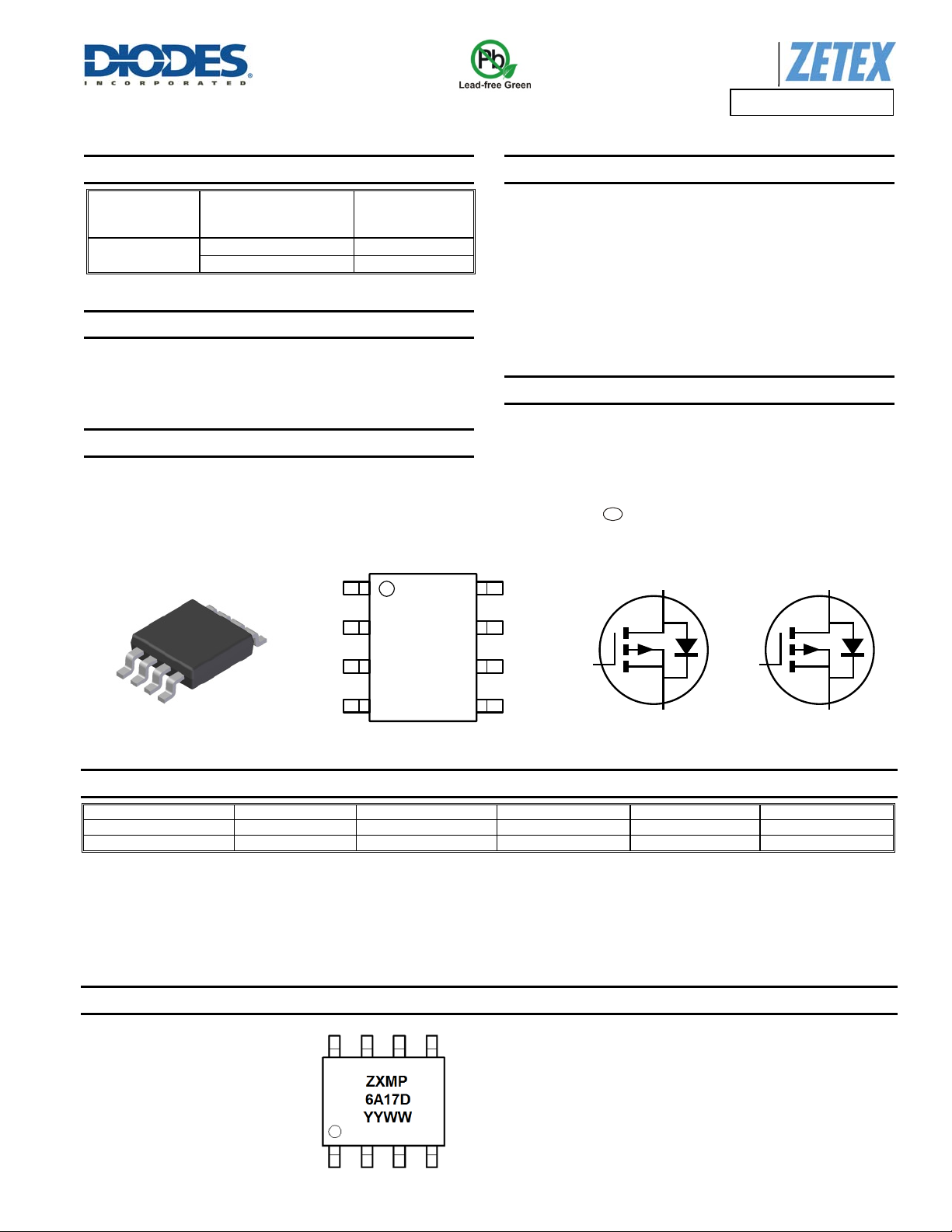
SO-8
G1
S2
G2
Top View
I
D
T
= 25°C
A
-3.4A
-2.8A
Top View
Features
Low On-Resistance
Fast Switching Speed
Low Threshold
Low Gate Drive
Low Profile SOIC Package
Totally Lead-Free & Fully RoHS compliant (Notes 1 & 2)
Halogen and Antimony Free. “Green” Device (Note 3)
Qualified to AEC-Q101 Standards for High Reliability
PPAP capable (Note 4)
Mechanical Data
Case: SO-8
Case Material: Molded Plastic, “Green” Molding Compound. UL
Flammability Classification Rating 94V-0
Moisture Sensitivity: Level 1 per J-STD-020
Terminals: Matte Tin Finish; Solderable per MIL-STD-202,
Method 208
Weight: 0.074 grams (approximate)
D1S1
e3
1
D1
D2
1
G2
D2
S1
Equivalent Circuit
Ordering Information (Notes 4 & 5)
Product Compliance Marking Reel size (inches) Tape width (mm) Quantity per reel
ZXMP6A17DN8TA AEC-Q101 ZXMP6A17D 7 12 500
ZXMP6A17DN8QTC Automotive ZXMP6A17D 13 12 2,500
Notes: 1. No purposely added lead. Fully EU Directive 2002/95/EC (RoHS) & 2011/65/EU (RoHS 2) compliant.
2. See http://www.diodes.com/quality/lead_free.html for more information about Diodes Incorporated’s definitions of Halogen- and Antimony-free, "Green"
and Lead-free.
3. Halogen- and Antimony-free "Green” products are defined as those which contain <900ppm bromine, <900ppm chlorine (<1500ppm total Br + Cl) and
<1000ppm antimony compounds.
4. Automotive products are AEC-Q101 qualified and are PPAP capable. Automotive, AEC-Q101 and standard products are electrically and thermally
5. For packaging details, go to our website at http://www.diodes.com/products/packages.html.
the same, except where specified. For more information, please refer to http://www.diodes.com/quality/product_compliance_definitions/.
Marking Information
ZXMP6A17D = Product Type Marking Code
YYWW = Date Code Marking
YY = Year (ex: 11 = 2011)
WW = Week (01 - 53)
2
S2
ZXMP6A17DN8
Document Number DS33588 Rev 4 - 2
1 of 8
www.diodes.com
August 2013
© Diodes Incorporated

A
f
Maximum Ratings (@T
= +25°C, unless otherwise specified.)
A
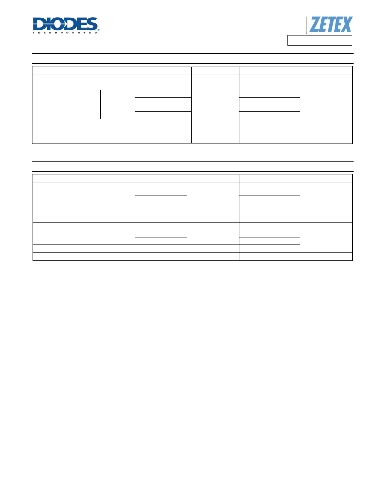
Characteristic Symbol Value Unit
Drain-Source voltage
Gate-Source voltage
V
DSS
V
GS
(Notes 7 & 9)
Continuous Drain current
V
GS
= 10V
(Notes 7 & 9)
I
D
TA = +70ºC
(Notes 6 & 9) -2.7
Pulsed Drain current (Notes 8 & 9)
Continuous Source current (Body diode) (Notes 7 & 9)
Pulsed Source current (Body diode) (Notes 8 & 9)
I
DM
I
S
I
SM
Thermal Characteristics (@T
ADVANCE INFORMATION
Characteristic Symbol Value Unit
= +25°C, unless otherwise specified.)
A
(Notes 6 & 9)
Power dissipation
Linear derating factor
(Notes 6 & 10)
P
D
(Notes 7 & 9)
(Notes 6 & 9)
Thermal Resistance, Junction to Ambient
(Notes 6 & 10) 70
R
θJA
(Notes 7 & 9) 60
Thermal Resistance, Junction to Lead (Notes 9 & 11)
Operating and storage temperature range
Notes: 6. For a device surface mounted on 25mm x 25mm x 1.6mm FR4 PCB with high cov erage of single sided 1oz copper, in still air conditions; the device is
measured when operating in a steady-state condition.
7. Same as note (6), except the device is measured at t 10 sec.
8. Same as note (6), except the device is pulsed with D = 0.02 and pulse width 300µs. The pulse current is limited by the maximum junction temperature.
9. For a dual device with one active die.
10. For a device with two active die running at equal power.
11. Thermal resistance from junction to solder-point.
R
θJL
T
, T
J
STG
Diodes Incorporated
ZXMP6A17DN8
-60 V
20
-3.42
-2.73
-15.6 A
-3.4 A
-15.6 A
1.25
10.0
1.81
14.5
2.15
17
100
51.68
-55 to 150 °C
Product Line o
V
A
W
mW/°C
°C/W
ZXMP6A17DN8
Document Number DS33588 Rev 4 - 2
2 of 8
www.diodes.com
August 2013
© Diodes Incorporated

A
f
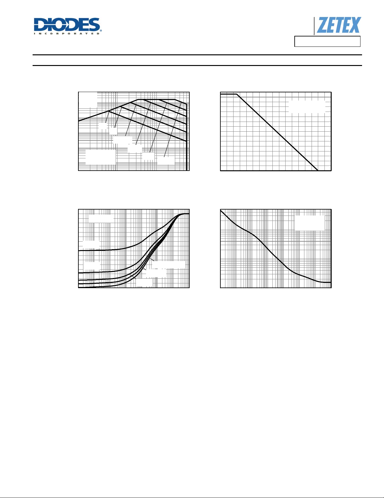
Thermal Characteristics
R
DS(on)
10
Limited
1
100m
10m
Drain Current (A)
D
1m
-I
100m 1 10
ADVANCE INFORMATION
DC
1s
100ms
Single Pulse
T
=25°C
amb
10ms
1ms
100µs
-VDS Drain-Source Voltage (V)
Safe Operating Area
Product Line o
Diodes Incorporated
1.6
1.4
1.2
1.0
0.8
0.6
0.4
0.2
0.0
0 20 40 60 80 100 120 140 160
Max Pow er Dissipat i o n (W )
Temperature (°C)
25mm x 25mm
1oz FR4
Derating Curve
ZXMP6A17DN8
80
70
60
50
40
30
20
10
Thermal Re sistance (°C/W)
T
=25°C
amb
D=0.5
D=0.2
0
100µ 1m 10m 100m 1 10 100 1k
Pulse Width (s)
Transient Thermal Impedance
D=0.1
Single Pulse
D=0.05
Single Pulse
T
=25°C
100
10
Maximum Power (W)
1
100µ 1m 10m 100m 1 10 100 1k
amb
Puls e Width (s)
Pulse Power Dissipation
ZXMP6A17DN8
Document Number DS33588 Rev 4 - 2
3 of 8
www.diodes.com
August 2013
© Diodes Incorporated
 Loading...