Diodes ZXMN3A14F User Manual

A
f
D
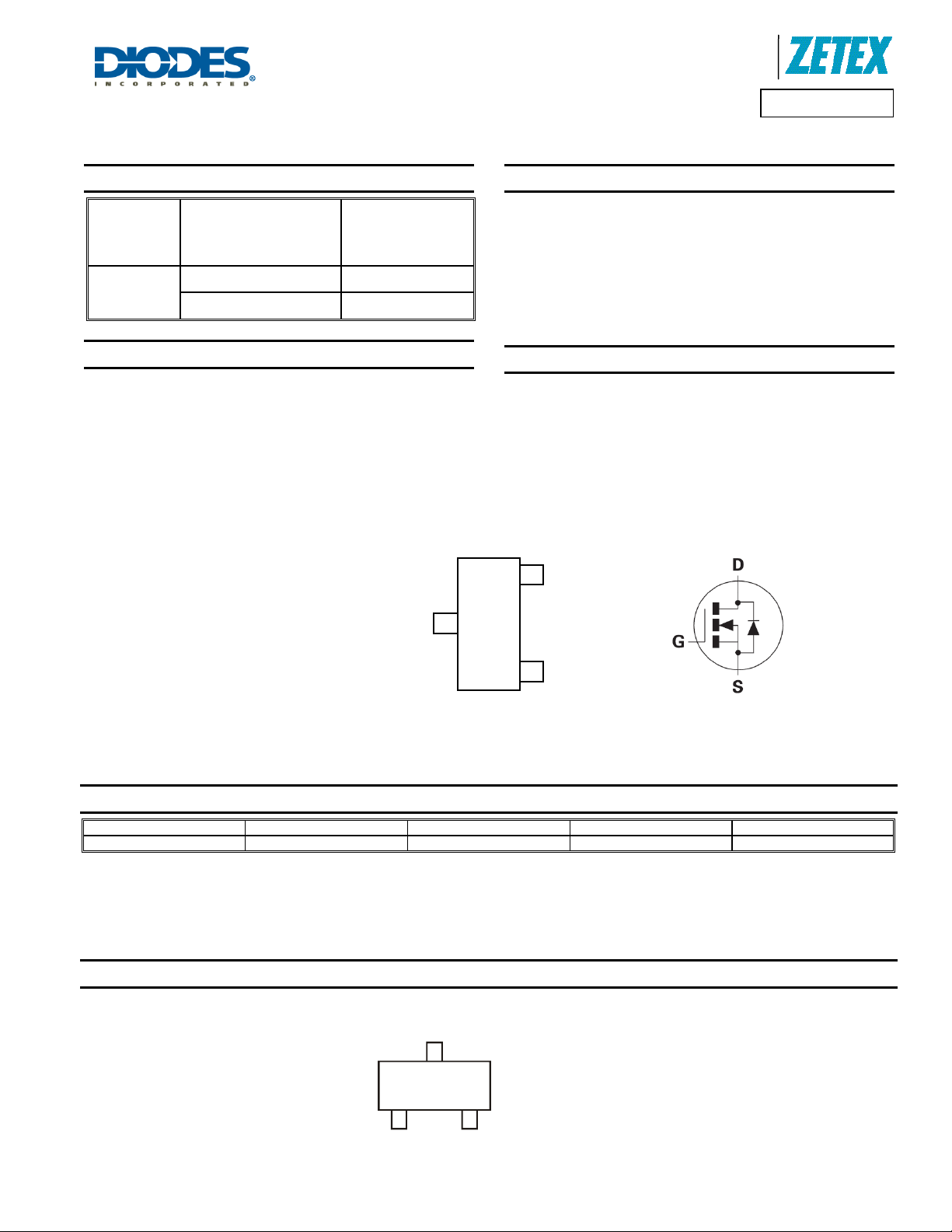
Product Summary
Max I
D
BV
Max R
DSS
30V
65mΩ @ V
95mΩ @ VGS = 4.5V
DS(on)
= 10V
GS
T
= 25°C
A
(Note 4)
3.2A
2.6A
Description and Applications
This MOSFET utilizes a unique structure that combines the benefits
of low on-resistance with fast switching speed, making it ideal for
high-efficiency power management applications.
• DC - DC converters
• Power management functions
• Disconnect switches
• Motor control
SOT23
Top View
Product Line o
Diodes Incorporated
ZXMN3A14F
30V N-CHANNEL ENHANCEMENT MODE MOSFET
Features and Benefits
• Low on-resistance
• Fast switching speed
• Low gate charge
• Low threshold
• Totally Lead-Free & Fully RoHS compliant (Note 1)
• Halogen and Antimony Free. “Green” Device (Note 2)
• Qualified to AEC-Q101 Standards for High Reliability
Mechanical Data
• Case: SOT23
• Case Material: Molded Plastic, UL Flammability Classification
Rating 94V-0
• Moisture Sensitivity: Level 1 per J-STD-020
• Terminals: Matte Tin Finish annealed over Copper leadframe
Solderable per MIL-STD-202, Method 208
• Weight: 0.008 grams (approximate)
S
G
Top View
Pin Out
Equivalent Circuit
Ordering Information (Note 3)
Product Marking Reel size (inches) Tape width (mm) Quantity per reel
ZXMN3A14FTA
Notes: 1. No purposely added lead. Fully EU Directive 2002/95/EC (RoHS) & 2011/65/EU (RoHS 2) compliant.
2. Halogen and Antimony free "Green” products are defined as those which contain <900ppm bromine, <900ppm chlorine (<1500ppm total Br + Cl) and
<1000ppm antimony compounds.
3. For more packaging details, go to our website at http://www.diodes.com.
314 7 8 3000 Units
Marking Information
ZXMN3A14F
Document Number DS33536 Rev. 2 - 2
314
www.diodes.com
314 = Product Type Marking Code
1 of 8
April 2012
© Diodes Incorporated

A
f
Product Line o
Diodes Incorporated
ZXMN3A14F
Maximum Ratings @T
= 25°C unless otherwise specified
A
Characteristic Symbol Value Units
Drain-Source Voltage
Gate-Source Voltage
Continuous Drain Current
V
GS
= 10V
TA = 70°C (Note 5)
Pulsed Drain Current (Note 6)
Continuous Source Current (Body Diode) (Note 5)
Pulsed Source Current (Body Diode) (Note 6)
(Note 5)
(Note 4)
V
DSS
V
GS
ID
I
DM
I
S
I
SM
30 V
±20 V
3.9
3.2
3.2
18 A
2.3 A
18 A
Thermal Characteristics @T
= 25°C unless otherwise specified
A
Characteristic Symbol Value Unit
Power Dissipation (Note 4)
Linear Derating Factor
Power Dissipation (Note 5)
Linear Derating Factor
Thermal Resistance, Junction to Ambient (Note 4)
Thermal Resistance, Junction to Ambient (Note 5)
Thermal Resistance, Junction to Leads (Note 7)
Operating and Storage Temperature Range
Notes: 4. For a device surface mounted on 25mm x 25mm FR4 PCB with high coverage of single sided 1oz copper, in still air conditions
5. For a device surface mounted on FR4 PCB measured at t ≤5 secs.
6. Repetitive rating 25mm x 25mm FR4 PCB, D=0.02 pulse width=300μs - pulse current limited by maximum junction temperature.
7. Thermal resistance from junction to solder-point (at the end of the drain lead).
R
R
R
T
J, TSTG
P
D
P
D
θJA
θJA
θJL
1
8
1.5
12
125 °C/W
83 °C/W
70.44 °C/W
-55 to +150 °C
A
W
mW/°C
W
mW/°C
ZXMN3A14F
Document Number DS33536 Rev. 2 - 2
2 of 8
www.diodes.com
April 2012
© Diodes Incorporated

A
f
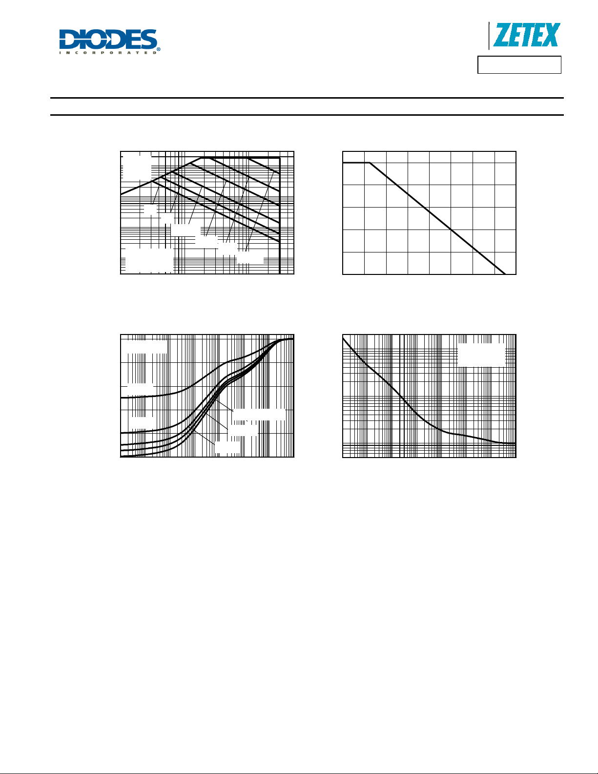
Thermal Characteristics
Product Line o
Diodes Incorporated
ZXMN3A14F
R
10
DS(on)
Limited
1
DC
amb
=25°C
1s
100ms
10ms
1ms
100µs
100m
Single Pulse
Drain Current (A)
10m
D
I
T
100m 1 10
VDS Drain-Source Voltage (V)
Safe Operating Area
T
=25°C
amb
100
D=0.5
50
D=0.2
0
100µ 1m 10m 100m 1 10 100 1k
Thermal Resistance (°C/W)
Pulse Width (s)
Single Pulse
D=0.05
D=0.1
1.0
0.8
0.6
0.4
0.2
0.0
0 20 40 60 80 100 120 140 160
Max Power Dissipation (W)
Temperature (°C)
Dera ting Curve
100
10
1
Maximum Power (W)
100µ 1m 10m 100m 1 10 100 1k
Pulse Width (s)
Single Pulse
T
=25°C
amb
Transient Thermal Impedance
ZXMN3A14F
Document Number DS33536 Rev. 2 - 2
3 of 8
www.diodes.com
Puls e Powe r Dissipat ion
April 2012
© Diodes Incorporated
 Loading...