

Page 1
f
D
30V N-CHANNEL ENHANCEMENT MODE MOSFET IN SOT89 PACKAGE
Product Summary
V
R
(BR)DSS
30V
Max
DS(on)
120mΩ @ V
180mΩ @ VGS = 4.5V
= 10V
GS
Description and Applications
This MOSFET has been designed to minimize the on-state resistance
) and yet maintain superior switching performance, making it
(R
DS(on)
ideal for high efficiency power management applications.
• DC-DC Converters
ADVANCE INFORMATION
• Power Management functions
• Motor control
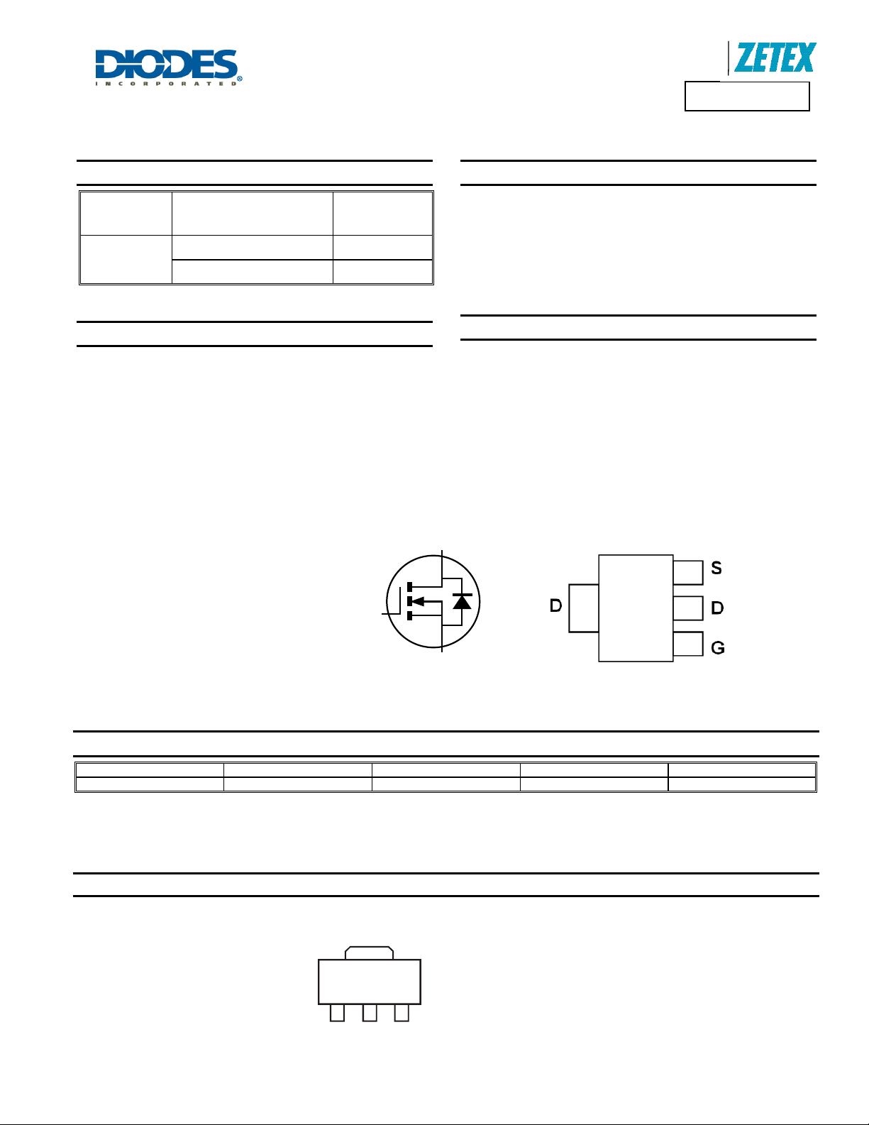
SOT89
Top View
Features and Benefits
I
max
D
= 25°C
T
A
(Note 5)
3.3A
2.7A
• Low On-Resistance
• Low Threshold
• Fast Switching Speed
• Low Gate Drive
• Lead Free/RoHS Compliant (Note 1)
• "Green" Device (Note 2)
• Qualified to AEC-Q101 Standards for High Reliability
Mechanical Data
• Case: SOT89
• Case Material: Molded Plastic, “Green” Molding Compound.
UL Flammability Classification Rating 94V-0
• Moisture Sensitivity: Level 1 per J-STD-020
• Terminals: Matte Tin Finish
• Weight: 0.052 grams (approximate)
G
S
Device symbol Pin-out Top
A Product Line o
Diodes Incorporated
ZXMN3A01Z
Ordering Information (Note 3)
Product Marking Reel size (inches) Tape width (mm) Quantity per reel
ZXMN3A01ZTA 1S8 7 12 1,000
Notes: 1. No purposefully added lead.
2. Diodes Inc’s “Green” Policy can be found on our website at http://www.diodes.com
3. For packaging details, go to our website at http://www.diodes.com
Marking Information
ZXMN3A01Z
Document number DS35722 Rev. 1 - 2
1S8
1S8 = Product type Marking Code
1 of 6
www.diodes.com
February 2012
© Diodes Incorporated
Page 2
f
P, P
T
RAN
N
T P
O
R
θ
R
CUR
RENT
T
R
T T
HER
R
TANC
Maximum Ratings @T
= 25°C unless otherwise specified
A
Characteristic Symbol Value Unit
Drain-Source Voltage
Gate-Source Voltage
Continuous Drain Current
Steady
State
@ V
@ V
@ V
= 10V ; T
GS
= 10V ; T
GS
= 10V ; T
GS
= 25°C (Note 5)
A
= 75°C (Note 5)
A
= 75°C (Note 4)
A
Pulsed Drain Current (Note 6)
Continuous Source Current (Body Diode) (Note 5)
Pulsed Source Current (Body Diode) (Note 6)
Thermal Characteristics @T
= 25°C unless otherwise specified
A
Characteristic Symbol Value Unit
Power Dissipation
Thermal Resistance, Junction to Ambient
(Note 4)
(Note 5) 2.12 W
(Note 4)
(Note 5) 59 °C/W
Operating and Storage Temperature Range
ADVANCE INFORMATION
Notes: 4. Device mounted on FR-4 substrate PC board, 2oz copper, with minimum recommended pad layout
5. Device mounted on 25mm X 25mm FR-4 substrate PC board with 2oz copper
6. Single pulse rating - 25mm x 25mm FR4 PCB, D=0.02, pulse width 300us – pulse width limited by maximum junction temperature.
1,000
100
A Product Line o
Diodes Incorporated
V
DSS
V
GSS
I
D
I
DM
I
S
I
SM
P
D
R
θJA
, T
T
J
STG
ZXMN3A01Z
30 V
±20 V
3.3
2.7
2.2
20 A
3.3 A
20 A
0.97 W
129 °C/W
-55 to +150 °C
A
(W)
IWE
SIE
EAK
(PK)
Single Pulse
R = 57C/W
θ
JA
R = r * R
θθ
JA(t) (t) JA
T - T = P * R
JA JA(t)
100
10
1
0.001 0.01 0.1 1 10 100 1,0000.0001
t1, PULSE DURATION TIME (sec)
Fig. 1 Single Pulse Maximum Power Dissipation
1
D = 0.7
E
D = 0.5
D = 0.3
ESIS
0.1
D = 0.1
MAL
D = 0.05
°
10
R
DS(on)
Limited
P = 10sWµ
(A)
1
AIN
D
I, D
0.1
T = 150°C
T = 25°C
V = 10V
Single Pulse
DUT on 1in. Board
0.01
0.1 1 10 100
D = 0.9
DC
P = 10s
W
P = 1s
W
P = 100ms
W
P = 10ms
W
P = 1ms
J(max)
A
GS
2
V , DRAIN-SOURCE VOLTAGE (V)
DS
W
P = 100µs
W
Fig. 2 SOA, Safe Operation Area
D = 0.02
0.01
D = 0.01
ANSIEN
D = 0.005
r(t),
Single Pulse
0.001
0.00001 0.0001 0.001 0.01 0.1 1 10 100 1,000
0.00001
t1, PULSE DURATION TIMES (sec)
R (t) = r(t) * R
θθ
JA JA
R = 57°C/W
θ
JA
Duty Cycle, D = t1/ t2
Fig. 3 Transi ent Thermal Resist ance
ZXMN3A01Z
Document number DS35722 Rev. 1 - 2
2 of 6
www.diodes.com
February 2012
© Diodes Incorporated
Page 3

f
)
g
g
g
g
r
r
)
r
)
R
CUR
RENT
R
CUR
R
T
)
Electrical Characteristics @T
= 25°C unless otherwise specified
A
Characteristic Symbol Min Typ Max Unit Test Condition
OFF CHARACTERISTICS
Drain-Source Breakdown Voltage
Zero Gate Voltage Drain Current TJ = 25°C I
Gate-Source Leakage
ON CHARACTERISTICS
Gate Threshold Voltage
Static Drain-Source On-Resistance (Note 7)
Forward Transconductance (Note 7 & 9)
Diodes Forward Voltage (Note 7)
DYNAMIC CHARACTERISTICS
Input Capacitance (Note 8 & 9)
Output Capacitance (Note 8 & 9)
ADVANCE INFORMATION
Reverse Transfer Capacitance (Note 8 & 9)
Gate Charge (Note 8 & 9)
Total Gate Charge (Note 8 & 9)
Gate-Source Charge (Note 8 & 9)
Gate-Drain Charge (Note 8 & 9)
Reverse Recovery Time (Note 9)
Reverse Recovery Charge (Note 9)
Turn-On Delay Time (Note 8 & 9)
Turn-On Rise Time (Note 8 & 9)
Turn-Off Delay Time (Note 8 & 9)
Turn-Off Fall Time (Note 8 & 9)
Notes: 7. Measured under pulsed conditions. Pulse width ≤ 300μs; duty cycle ≤2%.
8. Switching characteristics are independent of operating junction temperature.
9. For design aid only, not subject to production testing.
10
9
BV
I
V
GS(th
R
DS (ON)
g
V
C
C
C
Q
Q
t
D(on
t
D(off
DSS
DSS
GSS
FS
SD
iss
oss
rss
Q
Q
t
r
Q
t
t
A Product Line o
Diodes Incorporated
ZXMN3A01Z
30 - - V
s
d
r
f
- - 0.5
- - 100 nA
1 - - V
0.106 120
-
-
180
- 3.5 - S
- 0.85 0.95 V
- 186 - pF
- 48 - pF
- 29 - pF
- 2.6 - nC
- 5.0 - nC
- 0.8 - nC
- 1.2 - nC
17.7 ns
13.0 nC
- 2.6 - ns
- 4.1 - ns
- 13.5 - ns
- 3.6 - ns
10
9
VGS = 0V, ID = 250μA
μA
VDS = 30V, VGS = 0V
VGS = ±20V, VDS = 0V
VDS = VGS, ID = 250μA
= 10V, ID = 2.5A
V
mΩ
GS
= 4.5V, ID = 2A
V
GS
VDS = 4.5V, ID = 2.5A
TJ = 25°C, IS = 1.7A, VGS = 0V
= 25V, VGS = 0V,
V
DS
f = 1.0MHz
VGS = 4.5V, VDS = 15V, ID = 2.5A
V
= 10V, VDS = 15V,
GS
= 2.5A
I
D
= 25°C, IS = 2.5A,
T
J
di/dt = 100A/μs
V
= 10V, VDD = 15V,
GS
= 6Ω , ID = 2.5A
R
G
8
7
(A)
6
5
4
AIN
3
D
I, D
2
1
0
012345
V , DRAIN-SOURCE VOL TAGE (V)
DS
Fig. 4 Typical Output Characteristic, T = 25°C
A
8
7
(A
EN
6
5
4
AIN
3
D
I, D
2
1
0
0123 45
V , DRAIN-SOURCE VOL TAGE (V)
DS
Fig. 5 Typical Output Characteristic
, T = 150°C
A
ZXMN3A01Z
Document number DS35722 Rev. 1 - 2
3 of 6
www.diodes.com
February 2012
© Diodes Incorporated
Page 4

f
RAIN C
URREN
T
R
R
OUR
ON-R
R
RAIN-SOUR
CE O
N-R
TAN
C
C
UNC
TIO
C
P
C
T
C
F
GAT
THRESH
O
O
TAG
Diodes Incorporated
ZXMN3A01Z
A Product Line o
10
(A)
1
D
I, D
0.1
ADVANCE INFORMATION
T = 150°C
A
T = 125°C
A
T = 85°C
A
T = 25°C
A
T = -55°C
A
0123456
V , GATE-SOURCE VOLTAGE (V)
GS
Fig. 6 Typical Transfer Characteristics
10
Ω
ESISTANCE ( )
1
V = 2.5VGS V = 3.0VGS
CE
0.1
AIN-S
V = 3.5VGS
V = 4.0VGS V= 5.0V
GS
, D
DS(ON)
0.01
0.01 0.1 1 10
I , DRAIN-SOURCE CURRENT (A)
D
Fig. 7 Typical On-Resistance vs.
Drain Curr ent and Gate V oltage
V = 10VGS
1.4
Ω
E ( )
1.2
ESIS
1.0
V=
V
GS
0.8
, D
DS(ON)
0.6
-50 -25 0 25 50 75 100 125 150
T , JUNCTION TEMPERATURE ( C)
J
I = 250µA
D
DS
°
Fig. 8 On-Resistance Variation with Temperature
1,000
)
E (p
AN
I
A
A
N
, J
100
T
f = 1MHz
C
iss
C
oss
C
rss
10
T = 150°C
1
A
T= 25°C
A
0.1
S
I , SOURCE CURRENT (V)
0.01
0 0.2 0.4 0.6 0.8 1.0 1.4
V , SOURCE-DRAIN VOLTAG E (V)
SD
Fig. 9 Diode Forwar d Voltag e vs. Current
10
V = 15V
E (V)
DS
8
I= A
2.5
D
L
6
LD V
4
E
2
GS
V
1.2
10
0 5 10 15 20 25 30
V , DRAIN-SOURCE VOLTAGE (V)
DS
Fig. 10 Typical Junction Capacitance
ZXMN3A01Z
Document number DS35722 Rev. 1 - 2
4 of 6
www.diodes.com
0
0123456
, TOTAL GATE CHARGE
Q (nC)
g
Fig. 11 Gate Charge
February 2012
© Diodes Incorporated
Page 5

f
Package Outline Dimensions
E
ADVANCE INFORMATION
B1
8
°
(
4
X
Suggested Pad Layout
Y3
)
Y
B
X (3x)
D1
e1
D
e
X1
X2 (2x)
R
Y2
A Product Line o
Diodes Incorporated
ZXMN3A01Z
0
0
2
.
0
L
A
Y1
Y4
C
C
SOT89
Dim Min Max
A 1.40 1.60
B 0.44 0.62
H
B1 0.35 0.54
C 0.35 0.43
D 4.40 4.60
D1 1.52 1.83
E 2.29 2.60
e 1.50 Typ
e1 3.00 Typ
H 3.94 4.25
L 0.89 1.20
All Dimensions in mm
Dimensions Value (in mm)
X 0.900
X1 1.733
X2 0.416
Y 1.300
Y1 4.600
Y2 1.475
Y3 0.950
Y4 1.125
C 1.500
ZXMN3A01Z
Document number DS35722 Rev. 1 - 2
5 of 6
www.diodes.com
February 2012
© Diodes Incorporated
Page 6

f
DIODES INCORPORATED MAKES NO WARRANTY OF ANY KIND, EXPRESS OR IMPLIED, WITH REGARDS TO THIS DOCUMENT,
INCLUDING, BUT NOT LIMITED TO, THE IMPLIED WARRANTIES OF MERCHANTABILITY AND FITNESS FOR A PARTICULAR PURPOSE
(AND THEIR EQUIVALENTS UNDER THE LAWS OF ANY JURISDICTION).
Diodes Incorporated and its subsidiaries reserve the right to make modifications, enhancements, improvements, corrections or other changes
without further notice to this document and any product described herein. Diodes Incorporated does not assume any liability arising out of the
application or use of this document or any product described herein; neither does Diodes Incorporated convey any license under its patent or
trademark rights, nor the rights of others. Any Customer or user of this document or products described herein in such applications shall assume
all risks of such use and will agree to hold Diodes Incorporated and all the companies whose products are represented on Diodes Incorporated
website, harmless against all damages.
Diodes Incorporated does not warrant or accept any liability whatsoever in respect of any products purchased through unauthorized sales channel.
Should Customers purchase or use Diodes Incorporated products for any unintended or unauthorize d application, Customers shall indemnify and
hold Diodes Incorporated and its representatives harmless against all claims, damages, expenses, and attorney fees arising out of, directly or
indirectly, any claim of personal injury or death associated with such unintended or unauthorized application.
Products described herein may be covered by one or more United States, international or foreign patents pending. Product names and markings
noted herein may also be covered by one or more United States, international or foreign trademarks.
ADVANCE INFORMATION
Diodes Incorporated products are specifically not authorized for use as critical components in life support devices or systems without the express
written approval of the Chief Executive Officer of Diodes Incorporated. As used herein:
A. Life support devices or systems are devices or systems which:
1. are intended to implant into the body, or
labeling can be reasonably expected to result in significant injury to the user.
B. A critical component is any component in a life support device or system whose failure to perform can be reasonably expected to cause the
failure of the life support device or to affect its safety or effectiveness.
Customers represent that they have all necessary expertise in the safety and regulatory ramifications of their life support devices or systems, and
acknowledge and agree that they are solely responsible for all legal, regulatory and safety-related requirements concerning their products and any
use of Diodes Incorporated products in such safety-critical, life support devices or systems, notwithstanding any devices- or systems-related
information or support that may be provided by Diodes Incorporated. Further, Customers must fully indemnify Diodes Incorporated and its
representatives against any damages arising out of the use of Diodes Incorporated products in such safety-critical, life support devices or systems.
Copyright © 2012, Diodes Incorporated
www.diodes.com
2. support or sustain life and whose failure to perform when properly used in accordance with instructions for use provided in the
IMPORTANT NOTICE
LIFE SUPPORT
Diodes Incorporated
ZXMN3A01Z
A Product Line o
ZXMN3A01Z
Document number DS35722 Rev. 1 - 2
6 of 6
www.diodes.com
February 2012
© Diodes Incorporated
 Loading...