

Page 1
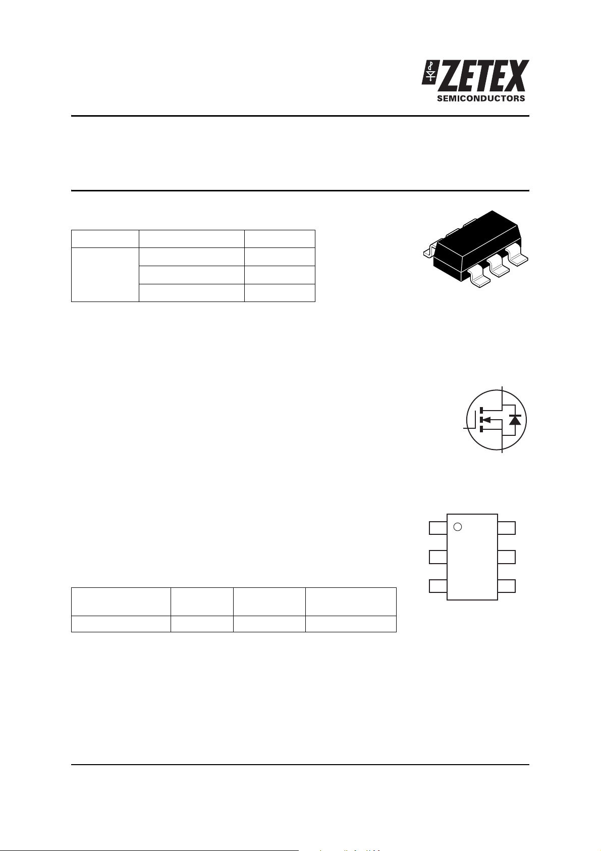
ZXMN2B03E6
20V SOT23-6 N-channel enhancement mode MOSFET
with low gate drive capability
Summary
V
(BR)DSS
20
R
0.040 @ V
0.055 @ V
0.075 @ V
(⍀)I
DS(on)
= 4.5V 5.4
GS
= 2.5V 4.6
GS
= 1.8V 4.0
GS
D
(A)
Description
This new generation trench MOSFET from Zetex features low onresistance achievable with low gate drive.
Features
• Low on-resistance
• Fast switching speed
• Low gate drive capability
• SOT23-6 package
Applications
• DC-DC converters
• Power management functions
• Disconnect switches
D
G
S
D
D
• Motor control
D
D
Ordering information
Device Reel size
(inches)
ZXMN2B03E6TA 7 8 3,000
Tape width
(mm)
Quantity per reel
G
Top view
S
Device marking
2B3
Issue 1 - September 2006 1 www.zetex.com
© Zetex Semiconductors plc 2006
Page 2
ZXMN2B03E6
Absolute maximum ratings
Parameter Symbol Limit Unit
Drain-source voltage V
Gate-source voltage V
Continuous drain current @ V
@ V
@ V
Pulsed drain current
(c)
= 4.5V; T
GS
= 4.5V; T
GS
= 4.5V; T
GS
Continuous source current (body diode)
(a)
(c)
Pulsed source current (body diode)
Power dissipation at T
amb
=25°C
(b)
amb
amb
amb
=25°C
=70°C
=25°C
(b)
(b)
(a)
DSS
I
I
DM
I
I
SM
P
GS
D
S
D
Linear derating factor 8.8 mW/°C
Power dissipation at T
amb
=25°C
(b)
P
D
Linear derating factor 13.7 mW/°C
Operating and storage temperature range T
j
, T
stg
20 V
± 8 V
5.4 A
4.3
4.3
26 A
2.8 A
26 A
1.1 W
1.7 W
-55 to +150 °C
Thermal resistance
Parameter Symbol Limit Unit
Junction to ambient
Junction to ambient
NOTES:
(a) For a device surface mounted on 25mm x 25mm FR4 PCB with high coverage of single sided 1oz copper, in still air
conditions.
(b) For a device surface mounted on FR4 PCB measured at t ⱕ5 sec.
(c) Repetitive rating - 25mm x 25mm FR4 PCB, D=0.02, pulse width 300s - pulse width limited by maximum junction
temperature.
(a)
(b)
R
R
⍜JA
⍜JA
113 °C/W
73 °C/W
Issue 1 - September 2006 2 www.zetex.com
© Zetex Semiconductors plc 2006
Page 3
Thermal characteristics
ZXMN2B03E6
Issue 1 - September 2006 3 www.zetex.com
© Zetex Semiconductors plc 2006
Page 4

ZXMN2B03E6
Electrical characteristics (at T
= 25°C unless otherwise stated)
amb
Parameter Symbol Min. Typ. Max. Unit Conditions
Static
Drain-source breakdown voltage V
Zero gate voltage drain current I
Gate-body leakage I
Gate-source threshold voltage V
Static drain-source on-state
(*)
resistance
Forward transconductance
Dynamic
(‡)
(*) (‡)
R
g
Input capacitance C
Output capacitance C
Reverse transfer capacitance C
Switching
(†) (‡)
Turn-on-delay time t
Rise time t
Turn-off delay time t
Fall time t
Total gate charge Q
Gate-source charge Q
Gate drain charge Q
(BR)DSS
DSS
GSS
GS(th)
DS(on)
fs
iss
oss
rss
d(on)
r
d(off)
f
g
gs
gd
20 V ID= 250A, VGS=0V
1 AVDS= 20V, VGS=0V
100 nA VGS=±8V, VDS=0V
0.4 1.0 V ID= 250A, VDS=V
0.040 ⍀ VGS= 4.5V, ID= 4.3A
0.055 ⍀ V
0.075 ⍀ V
= 2.5V, ID= 3.7A
GS
= 1.8V, ID= 3.2A
GS
13.5 S VDS= 10V, ID= 4.3A
1160 pF VDS= 10V, VGS=0V
210 pF
f=1MHz
136 pF
4.2 ns VDD= 10V, VGS= 4.5V
= 1A
I
6.2 ns
33.9 ns
D
R
G
≈ 6.0⍀
12.4 ns
14.5 nC VDS= 10V, VGS= 4.5V
= 4.3A
I
2nC
D
2.8 nC
Source-drain diode
Diode forward voltage
Reverse recovery time
(*)
(‡)
Reverse recovery charge
(‡)
V
SD
t
rr
Q
rr
0.67 0.95 V Tj=25°C, IS= 1.8A,
V
=0V
GS
10.8 ns Tj=25°C, IF= 2.8A,
3.4 nC
di/dt=100A/s
GS
NOTES:
(*) Measured under pulsed conditions. Pulse width ⱕ300s; duty cycle ⱕ2%.
(†) Switching characteristics are independent of operating junction temperature.
(‡) For design aid only, not subject to production testing.
Issue 1 - September 2006 4 www.zetex.com
© Zetex Semiconductors plc 2006
Page 5

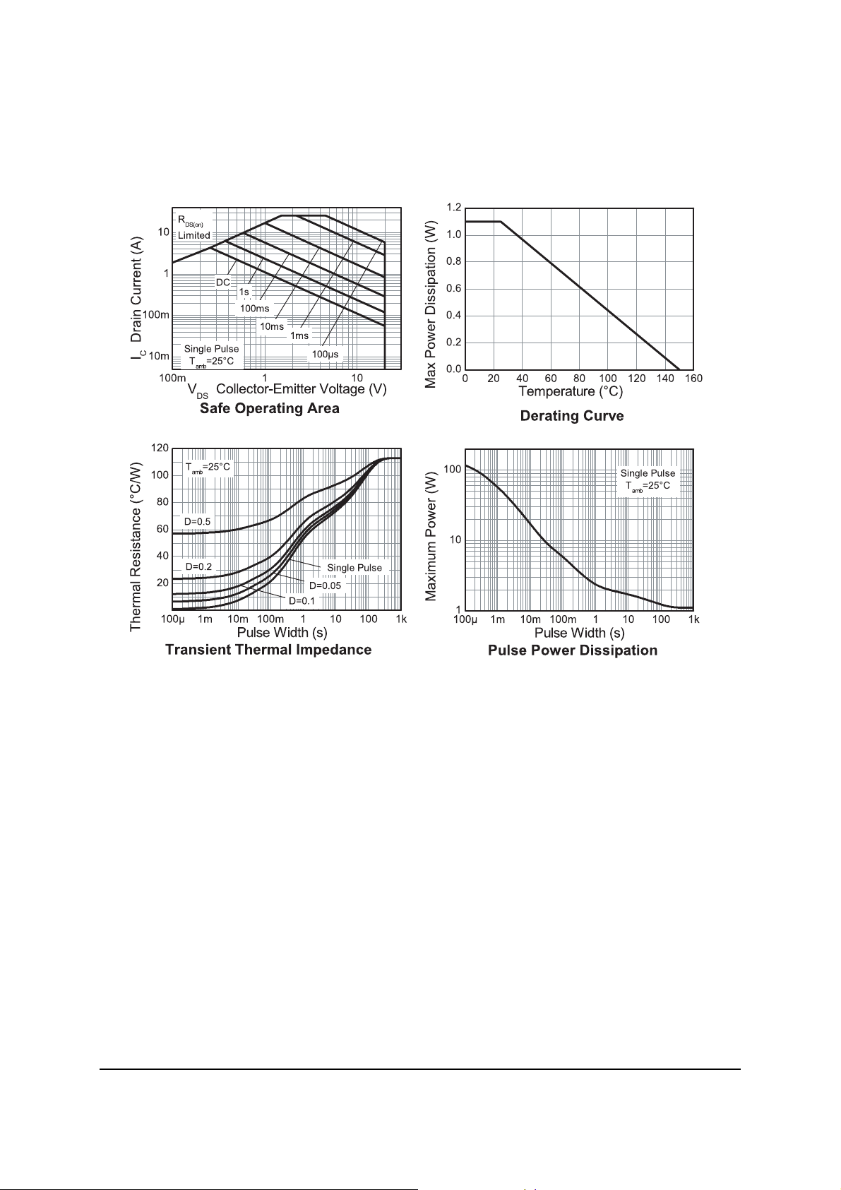
Typical characteristics
ZXMN2B03E6
Issue 1 - September 2006 5 www.zetex.com
© Zetex Semiconductors plc 2006
Page 6

Typical characteristics
Q
G
12V
ZXMN2B03E6
Current
regulator
50k
Same as
D.U.T
V
90%
10%
V
Q
V
GS
G
Q
GD
V
I
G
D.U.T
V
GS
DS
I
D
Charge
Basic gate charge waveform
DS
GS
t
d(on)tr
t
(on)
t
d(off)
t
r
t
(on)
Switching time waveforms
Gate charge test circuit
R
D
V
GS
R
G
V
Switching time test circuit
DS
V
CC
Issue 1 - September 2006 6 www.zetex.com
© Zetex Semiconductors plc 2006
Page 7

ZXMN2B03E6
Intentionally left blank
Issue 1 - September 2006 7 www.zetex.com
© Zetex Semiconductors plc 2006
Page 8

ZXMN2B03E6
Package outline - SOT23-6
DIM Millimeters Inches
Min. Max. Min. Max.
A 0.90 1.45 0.354 0.0570
A1 0.00 0.15 0.00 0.0059
A2 0.90 1.30 0.0354 0.0511
b 0.35 0.50 0.0078 0.0196
C 0.09 0.26 0.0035 0.0102
D 2.70 3.10 0.1062 0.1220
E 2.20 3.20 0.0866 0.1181
E1 1.30 1.80 0.0511 0.0708
L 0.10 0.60 0.0039 0.0236
e 0.95 REF 0.0374 REF
e1 1.90 REF 0.0748 REF
L 0° 30° 0° 30°
Note: Controlling dimensions are in millimeters. Approximate dimensions are provided in inches
Europe
Zetex GmbH
Kustermann-park
Balanstraße 59
D-81541 München
Germany
Telefon: (49) 89 45 49 49 0
Fax: (49) 89 45 49 49 49
europe.sales@zetex.com
For international sales offices visit www.zetex.com/offices
Zetex products are distributed worldwide. For details, see www.zetex.com/salesnetwork
This publication is issued to provide outline information only which (unless agreed by the company in writing) may not be used, applied or
reproduced for any purpose or form part of any order or contact or be regarded as a representation relating to the products or services concerned.
The company reserves the right to alter without notice the specification, design, price or conditions of supply of any product or service.
Americas
Zetex Inc
700 Veterans Memorial Highway
Hauppauge, NY 11788
USA
Telephone: (1) 631 360 2222
Fax: (1) 631 360 8222
usa.sales@zetex.com
Asia Pacific
Zetex (Asia Ltd)
3701-04 Metroplaza Tower 1
Hing Fong Road, Kwai Fong
Hong Kong
Telephone: (852) 26100 611
Fax: (852) 24250 494
asia.sales@zetex.com
Corporate Headquarters
Zetex Semiconductors plc
Zetex Technology Park, Chadderton
Oldham, OL9 9LL
United Kingdom
Telephone: (44) 161 622 4444
Fax: (44) 161 622 4446
hq@zetex.com
Issue 1 - September 2006 8 www.zetex.com
© Zetex Semiconductors plc 2006
 Loading...