Diodes ZXMN2AMC User Manual

A
f
Product Summary
max
I
D
V
(BR)DSS
20V
R
120mΩ @ V
300mΩ @ VGS= 2.5V
DS(on)
max
= 4.5V
GS
TA = 25°C
(Notes 4 & 7)
3.7A
2.3A
Description and Applications
This MOSFET has been designed to minimize the on-state resistance
) and yet maintain superior switching performance, making it
(R
DS(on)
ideal for high efficiency power management applications.
• DC-DC Converters
• Power management functions
• Disconnect switches
• Portable applications
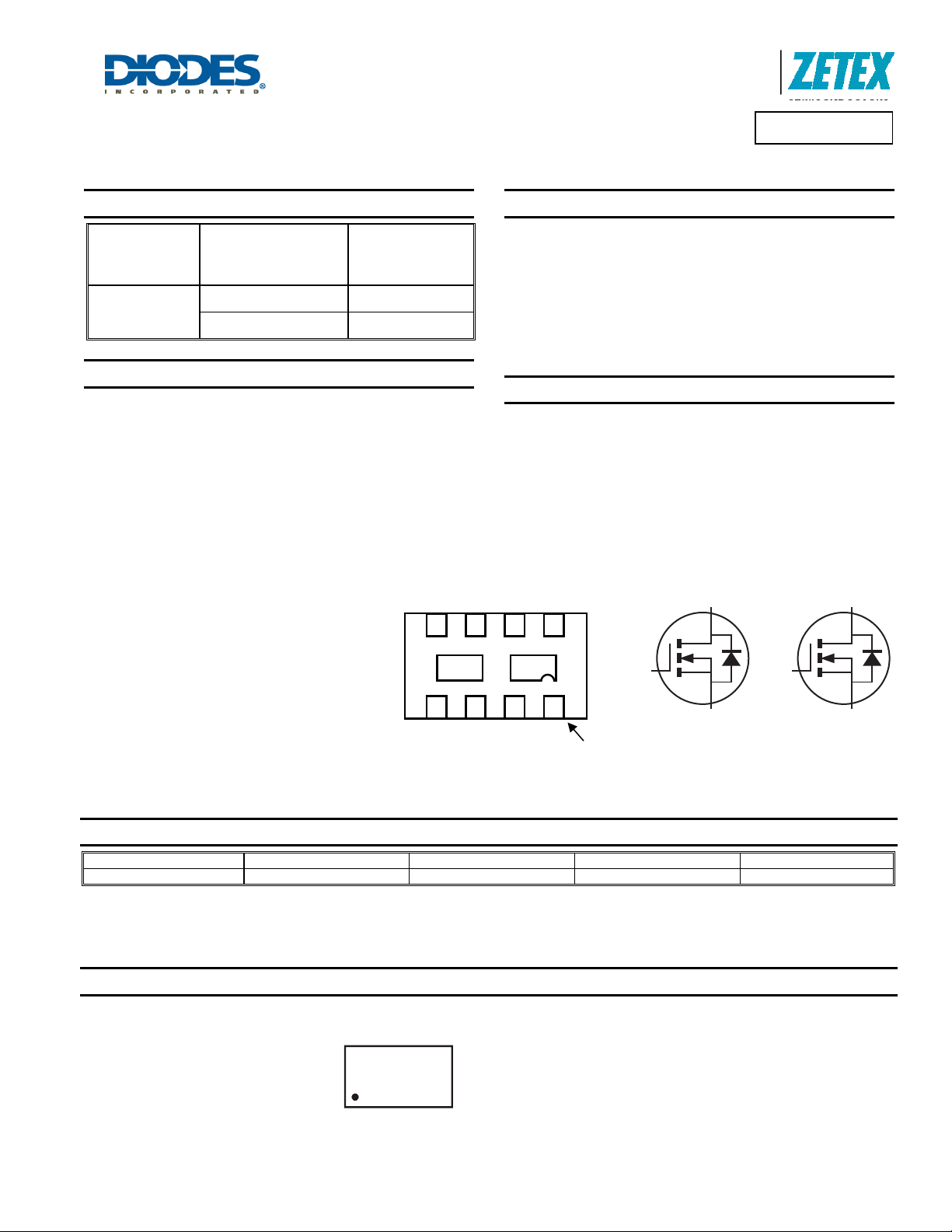
Top View
DFN3020B-8
D2 D2 D1 D1
D2
G2 S2 G1 S1
Bottom View
Product Line o
Diodes Incorporated
ZXMN2AMC
20V DUAL N-CHANNEL ENHANCEMENT MODE MOSFET
Features and Benefits
• Low profile package, for thin applications
• Low Rthj-a, thermally efficient package
• 6mm
• Low on-resistance
• Fast switching speed
• “Lead-Free”, RoHS Compliant (Note 1)
• Halogen and Antimony Free. "Green" Device (Note 2)
• Qualified to AEC-Q101 Standards for High Reliability
2
footprint, 50% smaller than TSOP6 and SOT23-6
Mechanical Data
• Case: DFN3020B-8
• Terminals: Pre-Plated NiPdAu leadframe
• Nominal package height: 0.8mm
• UL Flammability Rating 94V-0
• Moisture Sensitivity: Level 1 per J-STD-020
• Solderable per MIL-STD-202, Method 208
• Weight: 0.013 grams (approximate)
D2
S2
D1
Bottom View
Pin-Out
Pin 1
G1
D1
G2
S1
Equivalent Circuit
Ordering Information (Note 3)
Part Number Marking Reel size (inches) Tape width (mm) Quantity per reel
ZXMN2AMCTA DNA 7 8 3000
Notes: 1. No purposefully added lead
2. Diodes Inc's "Green" policy can be found on our website at http://www.diodes.com.
3. For packaging details, go to our website at http://www.diodes.com.
Marking Information
DNA
ZXMN2AMC
Document number: DS35089 Rev. 1 - 2
DNA = Product Type Marking Code
Top View, Dot Denotes Pin 1
1 of 8
www.diodes.com
December 2010
© Diodes Incorporated

A
f
Product Line o
Diodes Incorporated
ZXMN2AMC
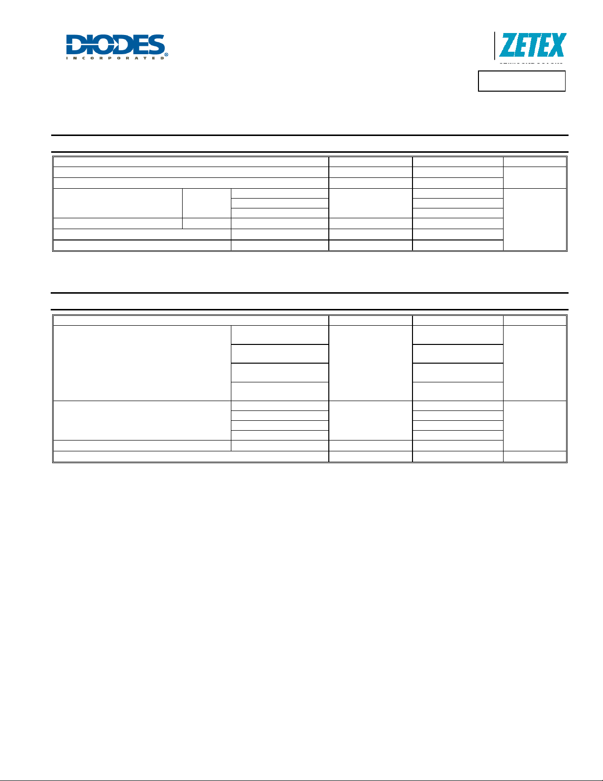
Maximum Ratings @T
= 25°C unless otherwise specified
A
Characteristic Symbol Value Unit
Drain-Source Voltage
Gate-Source Voltage
(Notes 4 & 7)
Continuous Drain Current VGS = 4.5V
TA = 70°C (Notes 4 & 7) 3.0
(Notes 3 & 7) 2.9
Pulsed Drain Current VGS = 4.5V (Notes 6 & 7)
Continuous Source Current (Body diode) (Notes 4 & 7)
Pulse Source Current (Body diode) (Notes 6 & 7)
V
V
DSS
GSS
I
I
DM
I
I
SM
D
S
20
±12
3.7
13
3.0
13
V
A
Thermal Characteristics @T
= 25°C unless otherwise specified
A
Characteristic Symbol Value Unit
1.50
12
2.45
19.6
1.13
9
1.70
13.6
83.3
W
mW/°C
°C/W
Power Dissipation
Linear Derating Factor
Thermal Resistance, Junction to Ambient
(Notes 3 & 7)
(Notes 4 & 7)
P
D
(Notes 5 & 7)
(Notes 5 & 8)
(Notes 3 & 7)
(Notes 4 & 7) 51.0
(Notes 5 & 7) 111
R
θJA
(Notes 5 & 8) 73.5
Thermal Resistance, Junction to Lead (Notes 7 & 9)
Operating and Storage Temperature Range
Notes: 3. For a device surface mounted on 28mm x 28mm (8 sq cm) FR4 PCB with high coverage of single sided 2oz copper, in still air conditions; the device is
measured when operating in a steady-state condition. The heatsink is split in half with the exposed drain pads connected to each half.
4. Same as note (3) except the device is measured at t < 5 sec.
5. Same as note (3), except the device is surface mounted on 31mm x 31mm (10 sq cm) FR4 PCB with high coverage of single sided 1oz copper.
6. Same as note (3), except the device is pulsed with D = 0.02 and pulse width 300 µs. The pulse current is limited by the maximum junction temperature.
7. For a dual device with one active die.
8. For dual device with 2 active die running at equal power.
9. Thermal resistance from junction to solder-point (at the end of the drain lead).
R
θJL
T
, T
J
STG
17.1
-55 to +150 °C
ZXMN2AMC
Document number: DS35089 Rev. 1 - 2
2 of 8
www.diodes.com
December 2010
© Diodes Incorporated

A
f
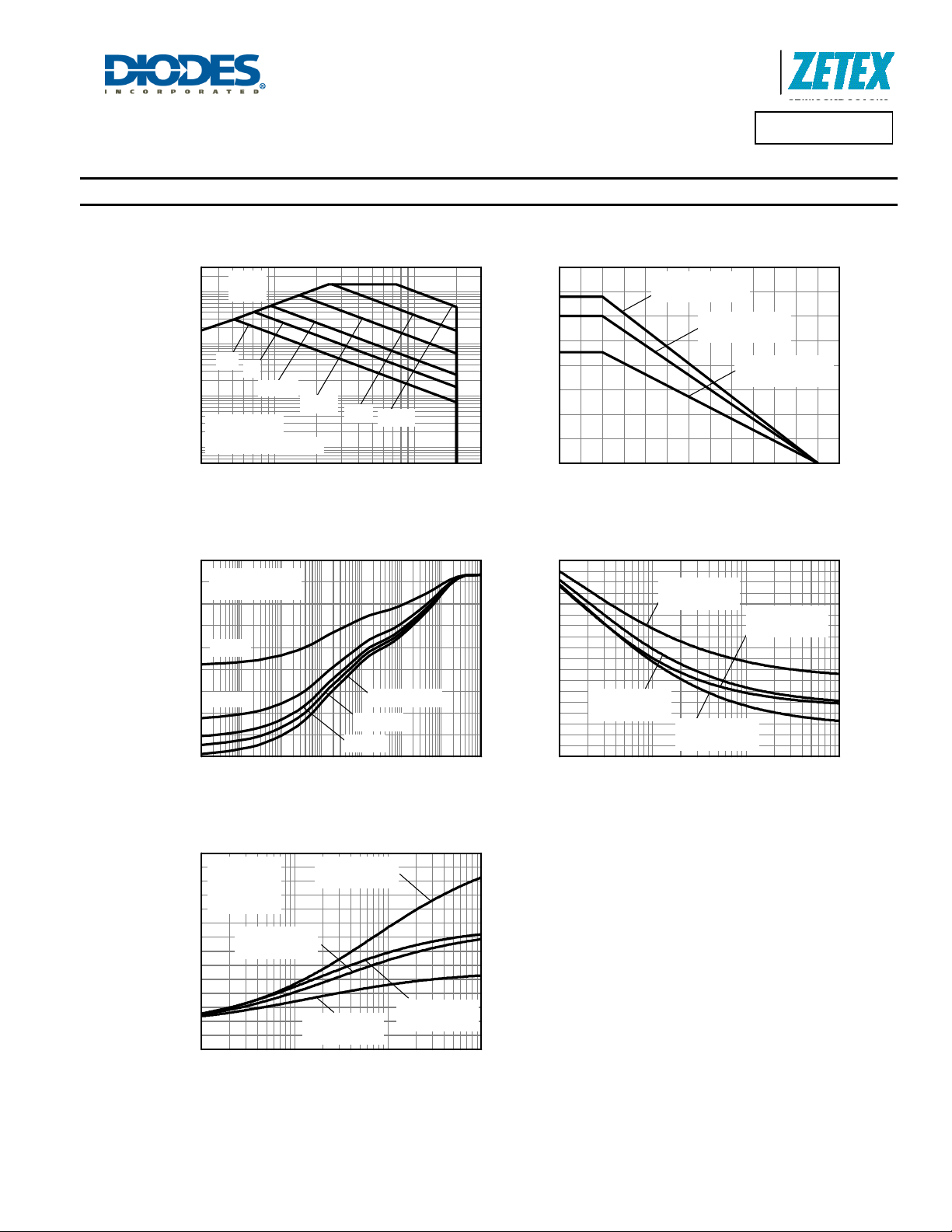
Thermal Characteristics
R
10
DS(on)
Limited
1
DC
1s
100m
Drain Current (A)
D
I
10m
8 sq cm 2oz Cu
One active die
Sing le Pulse, T
100ms
amb
110
VDS Drain-Source Voltage (V)
Safe Operating Area
=25°C
10ms
1ms
100us
Product Line o
Diodes Incorporated
2.0
1.5
1.0
0.5
0.0
0 25 50 75 100 125 150
Max Power Dissipation (W)
10 sq cm 1o z Cu
Two active die
8 sq cm 2oz Cu
One active die
10 sq cm 1oz Cu
One active die
Temperature (°C)
Derating Curve
ZXMN2AMC
8 sq cm 2oz Cu
80
One active die
60
D=0.5
40
D=0.2
20
Thermal Resistance (°C/W)
0
100µ 1m 10m 100m 1 10 100 1k
Single Pulse
D=0.05
D=0.1
Pulse Width (s)
Transient Thermal Impedance
3.5
T
=25°C
amb
3.0
T
=150°C
j max
Continuous
2.5
2.0
2oz Cu
One active die
1.5
1.0
Dissipation (W)
D
0.5
P
0.0
0.1 1 10 100
Board Cu Area (sqcm)
2oz Cu
Two active die
1oz Cu
One active die
1oz Cu
Two active die
Power Dissipation v Board Area
225
200
175
150
1oz Cu
One active die
1oz Cu
Two active die
125
100
75
50
25
Thermal Resistance (°C/W)
2oz Cu
One active die
0
0.1 1 10 100
2oz Cu
Two active die
Board Cu Area (sqcm)
Thermal Resistance v Board A rea
ZXMN2AMC
Document number: DS35089 Rev. 1 - 2
3 of 8
www.diodes.com
December 2010
© Diodes Incorporated
 Loading...