Diodes ZXMN2088DE6 User Manual

Part no.
ZXMN2088DE6
20V Dual SOT23-6 N-channel enhancement mode MOSFET
with low gate drive capability
Summary
V
(BR)DSS
20
R
0.200 @ VGS= 4.5V 2.1
0.240 @ VGS= 2.5V 1.9
DS(on)
(Ω)
I
(A)
D
0.310 @ VGS= 1.8V 1.7
Description
This new generation dual n-channel trench MOSFET from Zetex features low on-resistance
achievable with low gate drive.
Features
• Low on-resistance
• Low gate drive capability
• SOT23-6 (dual) package
Applications
• Power Management functions
• Disconnect switches
• Relay driving and load switching
Ordering information
Device Reel size
(inches)
Tape width
(mm)
Quantity
per reel
ZXMN2088DE6TA 7 8 3,000
Device marking
2088
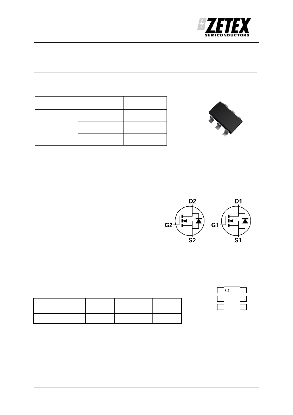
G1
S2
G2
Pinout – top view
D1
S1
D2
Issue 2 - June 2008 1 www.zetex.com
© Diodes Incorporated 2008 www.diodes.com

ZXMN2088DE6
Absolute maximum ratings
Parameter Symbol Limit Unit
Drain-Source voltage V
20 V
DSS
Gate-Source voltage VGS
Continuous Drain current @ VGS= 4.5V; TA=25°C
@ V
= 4.5V; TA=70°C
GS
@ VGS= 4.5V; TA=25°C
Pulsed Drain current
Power dissipation at TA =25°C
(c)
IDM 8 A
(a) (d)
(b) (d)
(b) (d)
(a) (d)
I
D
P
D
Linear derating factor
Power dissipation at TA =25°C
(a) (e)
P
D
Linear derating factor
Power dissipation at TA =25°C
(b) (d)
P
D
Linear derating factor
Operating and storage temperature range Tj, T
± 8
2.1
1.7
1.7
0.9
7.2
1.1
8.8
1.3
10.4
-55 to +150
stg
V
A
W
mW/°C
W
mW/°C
W
mW/°C
°C
Thermal resistance
Parameter Symbol Value Unit
Junction to Ambient
Junction to Ambient
(a) (d)
R
(a) (e)
R
139
θJA
113
θJA
°C/W
°C/W
Junction to Ambient
(b) (d)
R
96
θJA
°C/W
NOTES:
(a) For a device surface mounted on 25mm x 25mm FR4 PCB with high coverage of single sided 1oz copper, in
still air conditions.
(b) As above measured at t ≤ 5 sec.
(c) Repetitive rating - 25mm x 25mm FR4 PCB, D=0.02, pulse width 300us – pulse width limited by maximum
junction temperature.
(d) For device with one active die
(e) For device with two active die running at equal power.
Issue 2 – June 2008 2 www.zetex.com
© Diodes Incorporated 2008 www.diodes.com

ZXMN2088DE6
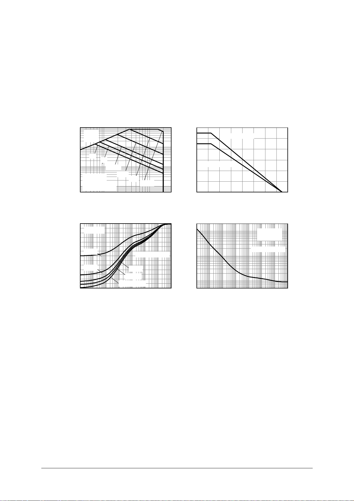
Thermal Characteristics
10
R
DS(on)
Limited
1
DC
1s
100m
Drain Current (A)
D
10m
I
Single Pul se
T
amb
1 Die Active (a)(d)
100ms
10ms
=25°C
110
1ms
100µs
VDS Drain-Source Voltage (V)
Safe Operating A rea
140
T
=25°C
amb
120
100
80
D=0.5
60
D=0.2
40
20
0
100µ 1m 10m 100m 1 10 100 1k
Thermal Resistance (°C/W)
Pulse Width (s)
1 Die Active (a)(d)
D=0.1
D=0.05
Single Pul se
Transient Thermal Impedance
1.2
1.0
0.8
0.6
1 Die Active (a)(d)
0.4
0.2
0.0
0 20 40 60 80 100 120 140 160
Max Power Dissipation (W)
2 Die Active (a)(e)
Temperature (°C)
Derating Curve
100
10
1
Maximum Power (W)
100µ 1m 10m 100m 1 10 100 1k
Pulse Width (s)
Single Pulse
T
=25°C
amb
1 Die Active (a)(d)
Pulse Power Dissipation
Issue 2 – June 2008 3 www.zetex.com
© Diodes Incorporated 2008 www.diodes.com
 Loading...