Diodes ZXMN10B08E6 User Manual

Product Summary
V
Max R
(BR)DSS
100V
DS(on)
230mΩ @ V
300mΩ @ VGS = 4.5V
= 10V
GS
Description and Applications
This new generation TRENCH MOSFETs from Diodes utilizes a
unique structure that combines the benefits of low on-resistance with
fast switching speed. This makes them ideal for high efficiency, low
voltage, power management applications.
• DC - DC Converters
• Power Management Functions
NEW PRODUCT
• Disconnect Switches
• Motor Control
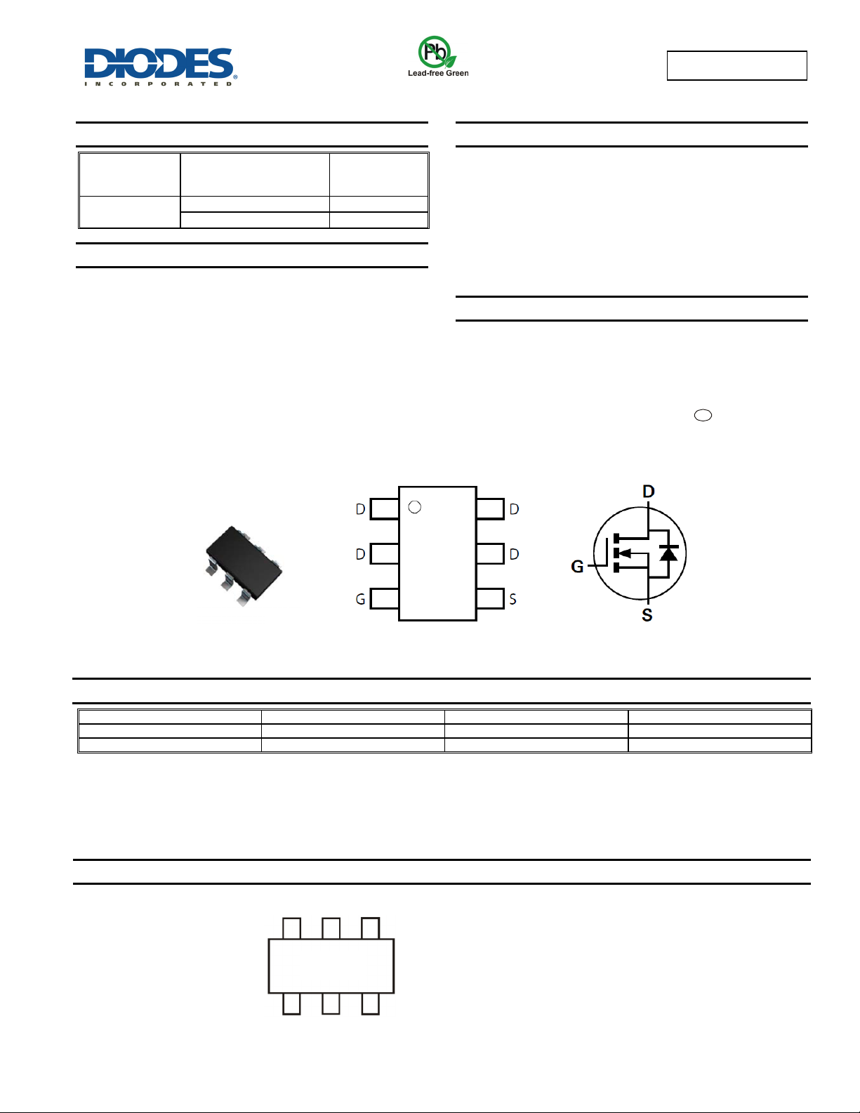
SOT26
Top View Pinout Top-view
Max I
D
TA = +25°C
(Note 6)
1.9A
1.68A
ZXMN10B08E6
100V N-CHANNEL ENHANCEMENT MODE MOSFET
Features and Benefits
• Low On-Resistance
• Fast Switching Speed
• Low Threshold
• Low Gate Drive
• SOT26 Package
• Lead-Free Finish; RoHS Compliant (Notes 1 & 2)
• Halogen and Antimony Free. “Green” Device (Note 3)
• Qualified to AEC-Q101 Standards for High Reliability
Mechanical Data
• Case: SOT26
• Case Material: Molded Plastic, “Green” Molding Compound.
UL Flammability Classification Rating 94V-0
• Moisture Sensitivity: Level 1 per J-STD-020
• Terminals: Finish – Matte Tin annealed over Copper leadframe
Solderable per MIL-STD-202, Method 208
• Weight: 0.015 grams (approximate)
Device Symbol
e3
Ordering Information (Note 4)
Part Number Reel Size (inch) Tape Width (mm) Quantity Per Reel
ZXMN10B08E6TA 7 8 3,000
ZXMN10B08E6TC 13 8 10,000
Notes: 1. EU Directive 2002/95/EC (RoHS) & 2011/65/EU (RoHS 2) compliant. All applicable RoHS exemptions applied.
2. See http://www.diodes.com/quality/lead_free.html for more information about Diodes Incorporated’s definitions of Halogen- and Antimony-free, "Green"
and Lead-free.
3. Halogen- and Antimony-free "Green” products are defined as those which contain <900ppm bromine, <900ppm chlorine (<1500ppm total Br + Cl) and
<1000ppm antimony compounds.
4. For packaging details, go to our website at http://www.diodes.com/products/packages.html.
Marking Information
ZXMN10B08E6
Datasheet Number: DS33570 Rev. 2 – 2
10B8
10B8 = Product Type Marking Code
1 of 7
www.diodes.com
May 2014
© Diodes Incorporated

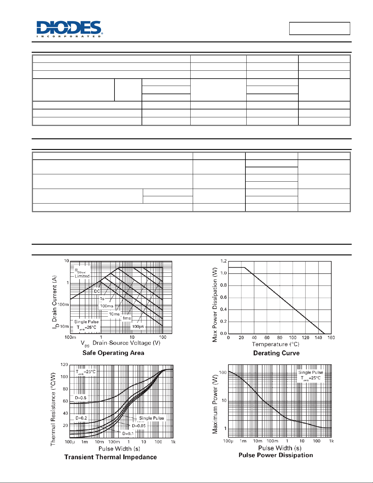
Maximum Ratings (@T
= +25°C, unless otherwise specified.)
A
Characteristic Symbol Value Unit
Drain-Source Voltage
Gate-Source Voltage
V
DSS
V
GS
(Note 6)
Continuous Drain Current
V
GS
= 10V
TA = +70°C (Note 6)
I
D
(Note 5) 1.6
Pulsed Drain Current (Note 7)
Continuous Source Current (Body Diode) (Note 6)
Pulsed Source Current (Body Diode) (Note 7)
Thermal Characteristics (@T
NEW PRODUCT
Characteristic Symbol Value Unit
= +25°C, unless otherwise specified.)
A
Power Dissipation (Note 5)
Linear Derating Factor
Power Dissipation (Note 6)
Linear Derating Factor
Thermal Resistance, Junction to Ambient
(Note 5)
(Note 6) 73
Operating and Storage Temperature Range
Notes: 5. For a device surface mounted on 25mm x 25mm FR4 PCB with high coverage of single sided 1oz copper, in still air conditions
6. For a device surface mounted on FR4 PCB measured at t ≤ 5 secs.
7. Repetitive rating 25mm x 25mm FR4 PCB, D = 0.02, pulse width 300µs - pulse width limited by maximum junction temperature. Refer to Transient
Thermal Impedance graph.
I
DM
I
S
I
SM
P
D
P
D
R
JA
θ
T
, T
J
STG
-55 to +150
Thermal Characteristics
ZXMN10B08E6
100 V
±20
1.9
1.5
9 A
2.5 A
9 A
1.1
8.8
1.7
13.6
113
V
A
W
mW/°C
W
mW/°C
°C/W
°C
ZXMN10B08E6
Datasheet Number: DS33570 Rev. 2 – 2
2 of 7
www.diodes.com
May 2014
© Diodes Incorporated

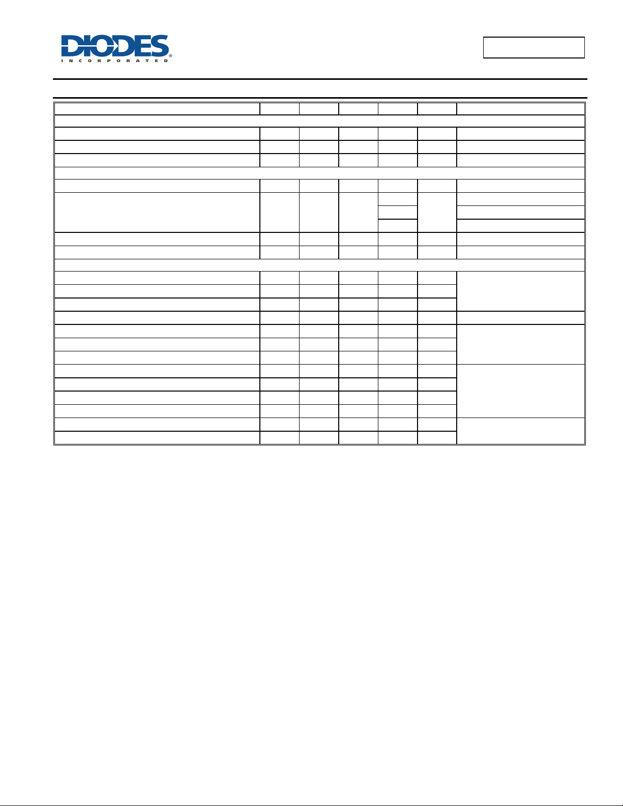
Electrical Characteristics (@T
= +25°C, unless otherwise specified.)
A
Characteristic Symbol Min Typ Max Unit Test Condition
OFF CHARACTERISTICS
Drain-Source Breakdown Voltage
Zero Gate Voltage Drain Current
Gate-Source Leakage
ON CHARACTERISTICS
Gate Threshold Voltage
Static Drain-Source On-Resistance (Note 8)
Forward Transconductance (Notes 8 & 10)
Diode Forward Voltage (Note 8)
NEW PRODUCT
DYNAMIC CHARACTERISTICS (Note 10)
Input Capacitance
Output Capacitance
Reverse Transfer Capacitance
Gate Charge (Note 9)
Total Gate Charge (Note 9)
Gate-Source Charge (Note 9)
Gate-Drain Charge (Note 9)
Turn-On Delay Time (Note 9)
Turn-On Rise Time (Note 9)
Turn-Off Delay Time (Note 9)
Turn-Off Fall Time (Note 9)
Reverse Recovery Time
Reverse Recovery Charge
Notes: 8. Measured under pulsed conditions. Width ≤ 300μs. Duty cycle ≤ 2%.
9. Switching characteristics are independent of operating junction temperature.
10. For design aid only, not subject to production testing.
ZXMN10B08E6
Datasheet Number: DS33570 Rev. 2 – 2
BV
DSS
I
DSS
I
GSS
V
GS(th)
R
⎯ ⎯
DS(ON)
g
fs
V
⎯
SD
C
⎯
iss
C
oss
C
⎯
rss
Q
⎯
g
Q
g
Q
⎯
gs
Q
⎯
gd
t
d(on)
t
⎯
r
t
⎯
d(off)
t
f
t
rr
Q
⎯
rr
www.diodes.com
100
⎯ ⎯
⎯ ⎯
1.0
⎯
0.85 0.95 V
497
⎯
⎯
⎯
12.1
⎯
3 of 7
⎯ ⎯
0.5 µA
100 nA
⎯
3.0 V
0.23
0.30
0.50
4.8
29
18
5.0
9.2
1.7
2.5
2.9
2.1
5.0
32
40
⎯
⎯
⎯
⎯
⎯
⎯
⎯
⎯
⎯
⎯
⎯
⎯
⎯
⎯
ZXMN10B08E6
V
ID = 250µA, VGS = 0V
VDS = 100V, VGS = 0V
VGS = ±20V, VDS = 0V
ID = 250µA, VDS = VGS
V
= 10V, ID = 1.6A
GS
Ω
V
= 4.5V, ID = 1.4A
GS
V
= 4.3V, ID = 1.1A
GS
S
VDS = 15V, ID = 1.6A
TJ = +25°C, IS = 2.0A, VGS = 0V
pF
V
= 50V, VGS = 0V
pF
pF
nC
nC
nC
nC
ns
ns
ns
ns
ns
nC
DS
f = 1.0MHz
VDS = 50V , VGS = 5V, ID = 1.6A
V
= 50V, VGS = 10V,
DS
= 1.6A
I
D
= 50V, ID = 1.0A,
V
DD
≅ 6.0Ω, VGS = 10V
R
G
= +25°C, IF = 1.7A,
T
J
di/dt = 100A/μs
May 2014
© Diodes Incorporated
 Loading...