Diodes ZXMN10A07F User Manual

A
f
D
Product Line o
Diodes Incorporated
100V N-CHANNEL ENHANCEMENT MODE MOSFET IN SOT23 PACKAGE
Product Summary
I
BV
R
DSS
100V
DS(ON) Max
700mΩ @ V
900mΩ @ VGS = 6V
= 10V
GS
D
TA = +25°C
(Note 6)
0.76A
0.67A
Description
This MOSFET has been designed to minimize the on-state resistance
) and yet maintain superior switching performance, making it
(R
DS(on)
ideal for high efficiency power management applications.
Applications
• DC-DC Converters
• Power Management Functions
• Motor Control
• Disconnect switches
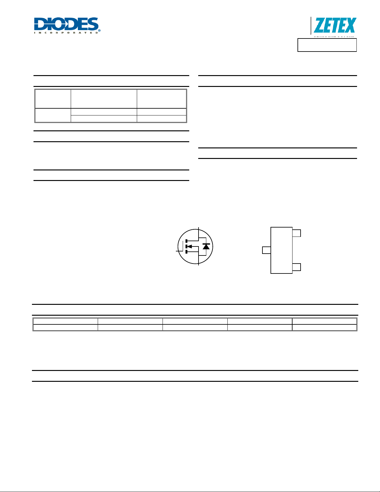
SOT23
G
Top View
ZXMN10A07F
Features
• Low On-Resistance
• Low Threshold
• Fast Switching Speed
• Low Gate Drive
• Totally Lead-Free & Fully RoHS Compliant (Notes 1 & 2)
• Halogen and Antimony Free. “Green” Device (Note 3)
• Qualified to AEC-Q101 Standards for High Reliability
Mechanical Data
• Case: SOT23
• Case Material: Molded Plastic, “Green” Molding Compound. UL
Flammability Classification Rating 94V-0
• Moisture Sensitivity: Level 1 per J-STD-020
• Terminals: Matte Tin Finish
• Weight: 0.008 grams (approximate)
D
S
Device Symbol
Top View
Pin-Out
S
G
Ordering Information (Note 4)
Part Number Marking Reel size (inches) Tape width (mm) Quantity per reel
ZXMN10A07FTA 7N1 7 8 3,000
Notes: 1. No purposely added lead. Fully EU Directive 2002/95/EC (RoHS) & 2011/65/EU (RoHS 2) compliant.
3. Halogen and Antimony free "Green” products are defined as those which contain <900ppm bromine, <900ppm chlorine (<1500ppm total Br + Cl) and
4. For packaging details, go to our website at http://www.diodes.com
2. See http://www.diodes.com for more information about Diodes Incorporated’s definitions of Halogen and Antimony free,"Green" and Lead-Free.
<1000ppm antimony compounds.
Marking Information
ZXMN10A07F
Document number: DS33564 Rev. 6 - 2
www.diodes.com
7N1 = Product Type Marking Code
1 of 7
August 2012
© Diodes Incorporated

A
f
Product Line o
Diodes Incorporated
Maximum Ratings (@T
= +25°C, unless otherwise specified.)
A
Characteristic Symbol Value Unit
Drain-Source Voltage
Gate-Source Voltage
Continuous Drain Current
Steady
State
Pulsed Drain Current (Note 7)
Continuous Source Current (Body Diode) (Note 6)
Pulsed Source Current (Body Diode) (Note 7)
@ V
@ V
@ V
@ V
= 10V; T
GS
= 10V; T
GS
= 10V; T
GS
= 10V; T
GS
= +25°C (Note 6)
A
= +70°C (Note 6)
A
= +100°C (Note 6)
A
= +25°C (Note 5)
A
V
DSS
V
GSS
I
D
I
DM
I
S
I
SM
100 V
±20 V
0.8
0.6
0.5
0.7
3.5 A
0.5 A
3.5 A
Thermal Characteristics (@T
= +25°C, unless otherwise specified.)
A
Characteristic Symbol Value Unit
Power Dissipation (Note 5)
Power Dissipation (Note 6)
Thermal Resistance, Junction to Ambient (Note 5)
Thermal Resistance, Junction to Ambient (Note 6)
Thermal Resistance, Junction to Leads (Note 8)
Operating and Storage Temperature Range
Notes: 5. For a device surface mounted on 25mm x 25mm FR4 PCB with high coverage of single sided 1oz copper, in still air conditions.
6. For a device surface mounted on FR4 PCB measured at t ≤ 10 sec.
7. Repetitive rating - 25mm x 25mm FR4 PCB, D = 0.02, pulse width 300s – pulse width limited by maximum junction temperature.
8. Thermal resistance from junction to solder-point (at the end of the drain lead).
P
D
P
D
R
JA
R
JA
R
JL
, T
T
J
STG
625 mW
806 mW
200 °C/W
155 °C/W
194 °C/W
-55 to +150 °C
ZXMN10A07F
A
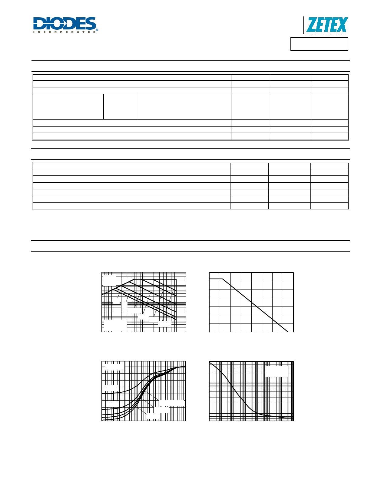
Thermal Characteristics
R
DS(on)
Limited
1
100m
10m
Drain Current (A)
D
I
200
150
100
Thermal Resistance (°C/W)
1m
DC
Single Pulse
T
=25°C
amb
110100
VDS Drain-Source Voltage (V)
Safe Operating Area
T
=25°C
amb
D=0.5
D=0.2
50
0
100µ 1m 10m 100m 1 10 100 1k
Transient Thermal Impedance
1s
100ms
10ms
Pulse Width (s)
1ms
D=0.1
100µs
Single Pulse
D=0.05
0.7
0.6
0.5
0.4
0.3
0.2
0.1
0.0
0 20 40 60 80 100 120 140 160
Max Power Dissipat i on (W)
Temperature (°C)
Derating Curve
Single Pulse
T
=25°C
amb
10
1
Maximum Power (W)
100µ 1m 10m 100m 1 10 100 1k
Pulse Width (s )
Pulse P ower Dis sipation
ZXMN10A07F
Document number: DS33564 Rev. 6 - 2
2 of 7
www.diodes.com
August 2012
© Diodes Incorporated

A
f
)
g
g
g
g
r
r
)
r
)
Product Line o
Diodes Incorporated
Electrical Characteristics (@T
= +25°C, unless otherwise specified.)
A
ZXMN10A07F
Characteristic Symbol Min Typ Max Unit Test Condition
OFF CHARACTERISTICS
Drain-Source Breakdown Voltage
Zero Gate Voltage Drain Current TJ = +25°C I
Gate-Source Leakage
BV
I
DSS
DSS
GSS
100 — — V
— — 1.0 µA
— — 100 nA
VGS = 0V, ID = 250A
VDS = 100V, VGS = 0V
VGS = ±20V, VDS = 0V
ON CHARACTERISTICS
Gate Threshold Voltage
Static Drain-Source On-Resistance (Note 9)
Forward Transconductance (Notes 9 & 11)
Diodes Forward Voltage (Note 9)
V
GS(th
R
DS (ON)
V
g
fs
SD
2 — 4 V
—
540 700
700 900
— 1.6 — S
— 0.85 0.95 V
VDS = VGS, ID = 250A
V
= 10V, ID = 1.5A
m
GS
V
= 6V, ID = 1A
GS
VDS = 15V, ID = 1A
TJ = +25°C, IS = 1.5A, VGS = 0V
DYNAMIC CHARACTERISTICS
Input Capacitance (Notes 10 & 11)
Output Capacitance (Notes 10 & 11)
Reverse Transfer Capacitance (Notes 10 & 11)
Gate Resistance (Notes 10 & 11)
Total Gate Charge (Notes 10 & 11)
Gate-Source Charge (Notes 10 & 11)
Gate-Drain Charge (Notes 10 & 11)
Reverse Recovery Time (Note 11)
Reverse Recovery Charge (Note 11)
Turn-On Delay Time (Notes 10 & 11)
Turn-On Rise Time (Notes 10 & 11)
Turn-Off Delay Time (Notes 10 & 11)
Turn-Off Fall Time (Notes 10 & 11)
Notes: 9. Measured under pulsed conditions. Pulse width ≤ 300µs; duty cycle ≤ 2%.
10. Switching characteristics are independent of operating junction temperature.
11. For design aid only, not subject to production testing.
ZXMN10A07F
Document number: DS33564 Rev. 6 - 2
C
iss
C
oss
C
rss
R
Q
Q
s
Q
d
t
r
Q
r
t
D(on
t
t
D(off
t
f
www.diodes.com
— 138 280
— 12 25
— 6 12
— 2 4
— 2.9 6
— 0.7 1.5
— 1 2
— 27 60 ns
— 12 — nC
— 1.8 —
— 1.5 —
— 4.1 —
— 2.1 —
3 of 7
V
= 50V, VGS = 0V,
pF
DS
f = 1.0MHz
f = 1MHz, VGS = 0V, VDS = 0V
V
= 10V, VDS = 50V,
nC
GS
I
= 1A
D
T
= +25°C, IF = 1.8A,
J
di/dt = 100A/µs
V
= 10V, VDD = 50V,
ns
GS
= 6 , ID = 1A
R
G
August 2012
© Diodes Incorporated
 Loading...