Diodes ZXMHC6A07N8 User Manual

A
Product Line o
f
Diodes Incorporated
ZXMHC6A07N8
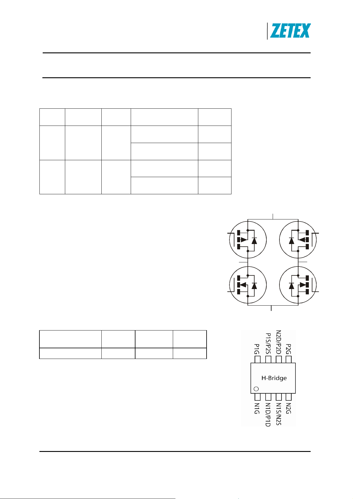
60V SO8 Complementary enhancement mode MOSFET H-Bridge
Summary
I
Device V
Q
(BR)DSS
R
G
DS(on)
= 25°C
T
A
D
0.25Ω @ V
= 10V 1.8A
GS
N-CH 60V 3.2nC
0.35Ω @ VGS= 4.5V 1.5A
0.40Ω @ V
= -10V -1.4A
GS
P-CH -60V 5.1nC
0.60Ω @ VGS= -4.5V -1.2A
Description
This new generation complementary MOSFET H-Bridge
features low on-resistance achievable with low gate drive.
Features
• 2 x N + 2 x P channels in a SOIC package
Applications
• DC Motor control
• DC-AC Inverters
P1S/P2S
P1G P2G
P1D/N1D
N1S/N2S
P2D/N2D
N2G N1G
Ordering information
Device Reel size
(inches)
ZXMHC6A07N8TC 13 12 2,500
Tape width
(mm)
Quantity
per reel
Device marking
ZXMHC
6A07
Issue 1.0 - March 2009 1
© Diodes Incorporated
www.diodes.com

Absolute maximum ratings
ZXMHC6A07N8
Parameter Symbol N-
channel P-channel
Drain-Source voltage
Gate-Source voltage
(c)
(b)
(b)
(a)
(f)
Continuous Drain current @ VGS= 10V; TA=25°C
@ V
@ V
= 10V; TA=70°C
GS
= 10V; TA=25°C
GS
@ VGS= 10V; TL=25°C
Pulsed Drain current @ VGS= 10V; TA=25°C
Continuous Source current (Body diode) at TA =25°C
Pulsed Source current (Body diode) at TA =25°C
Power dissipation at TA =25°C
(a)
(c)
DSS
V
GS
I
D
I
DM
(b)
I
S
I
SM
P
D
60 -60 V
±20 ±20
1.80
1.40
1.39
1.42
7.10 -6.03 A
1.00 -1.00 A
7.10 -6.03 A
V
Linear derating factor
Power dissipation at TA =25°C
(b)
P
D
Linear derating factor
Power dissipation at TL =25°C
(f)
P
D
Linear derating factor
, T
Operating and storage temperature range
T
j
stg
-1.42
-1.28
-1.28
-1.33
0.87
6.94
1.36
10.9
0.90
7.19
-55 to 150
Unit
V
A
W
mW/°C
W
mW/°C
W
mW/°C
°C
Thermal resistance
Parameter Symbol Value Unit
(f)
(a)
(b)
(d)
(e)
Junction to ambient
Junction to ambient
Junction to ambient
Junction to ambient
Junction to lead
NOTES:
(a) For a device surface mounted on 25mm x 25mm x 1.6mm FR4 PCB with high coverage of single sided 1oz copper, in still
air conditions with the heat-sink split into two equal areas (one for each drain connection); the device is measured when
operating in a steady-state condition with one active die.
(b) Same as note (a), except the device is measured at t ≤ 10 sec.
(c) Same as note (a), except the device is pulsed with D= 0.02 and pulse width 300 µs. The pulse current is limited by the
maximum junction temperature.
(d) For a device surface mounted on 50mm x 50mm x 1.6mm FR4 PCB with high coverage of single sided 2oz copper, in still
air conditions with the heat-sink split into two equal areas (one for each drain connection); the device is measured when
operating in a steady-state condition with one active die.
(e) For a device surface mounted on minimum copper 1.6mm FR4 PCB, in still air conditions; the device is measured when
operating in a steady-state condition with one active die.
(f) Thermal resistance from junction to solder-point (at the end of the drain lead); the device is operating in a steady-state
condition with one active die.
R
R
R
R
R
θJA
θJA
θJA
θJA
θJL
144
92
106
254
139
°C/W
°C/W
°C/W
°C/W
°C/W
Issue 1.0 - March 2009 2
© Diodes Incorporated
www.diodes.com

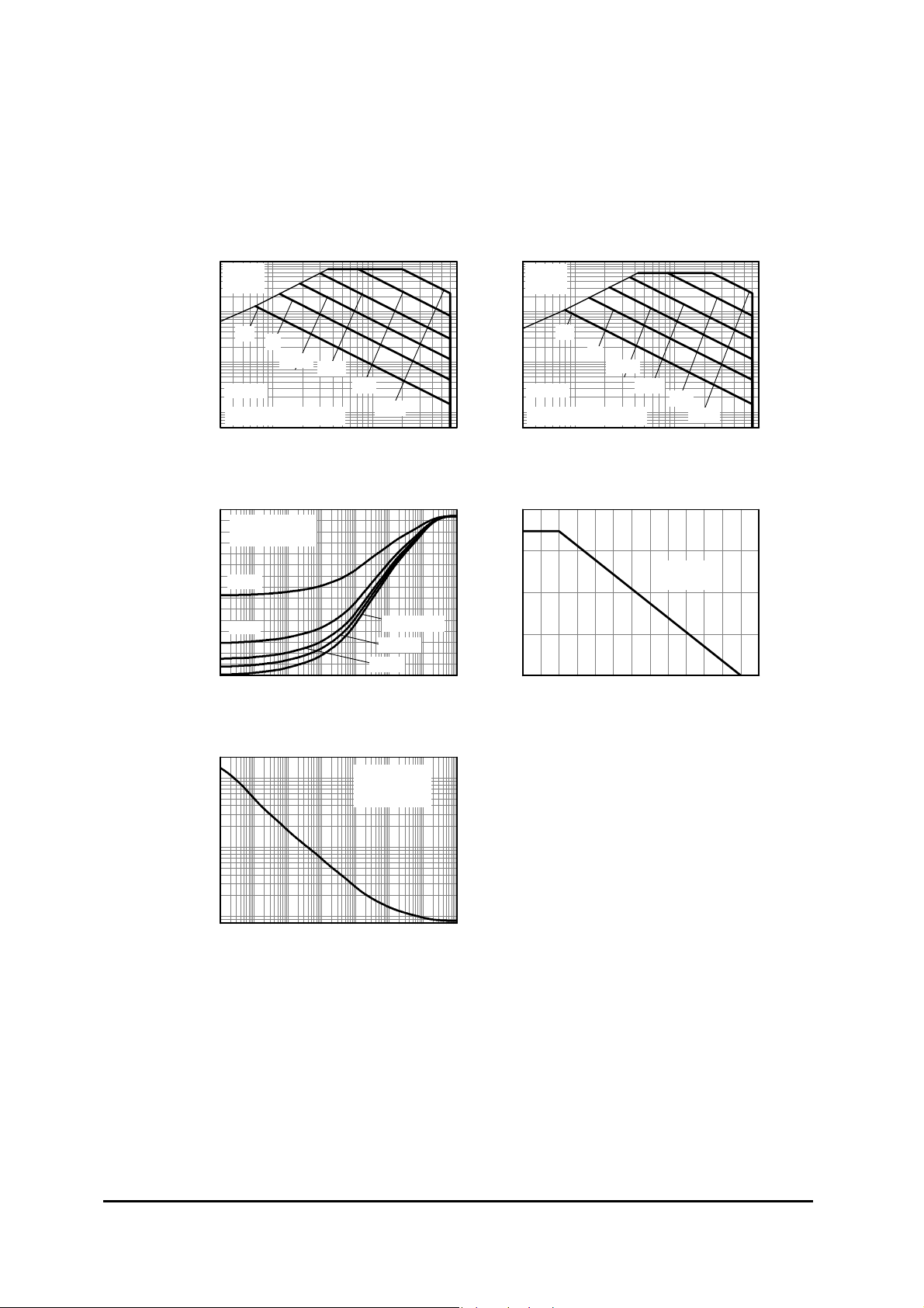
Thermal characteristics
ZXMHC6A07N8
10
R
DS(ON)
Limited
1
DC
1s
100m
Drain Current (A)
D
10m
I
Note (a)
Single Pulse, T
100ms
10ms
1ms
=25°C
amb
110
100us
VDS Drain-Source Voltage (V)
N-channel Safe Operating Area
140
One Active Die
25 x 25mm 1oz
120
100
D=0.5
80
60
D=0.2
40
20
Thermal Resistance (°C/W)
0
100µ 1m 10m 100m 1 10 100 1k
Single Pulse
D=0.05
D=0.1
Pulse Width (s)
Transient Thermal Impedan ce
10
R
DS(ON)
Limited
1
DC
100m
Drain Current (A)
D
10m
-I
Note (a)
Single Pulse, T
1s
100ms
10ms
1ms
=25°C
amb
110
100us
-VDS Drain-Source Voltage (V)
P-channel Safe Operating Area
1.0
Any one
0.5
0.0
0 25 50 75 100 125 150
Max Power Dissipation (W)
Temperature (°C)
active die
Derating Curve
100
10
Maximum Power (W)
1
100µ 1m 10m 100m 1 10 100 1k
One Active Die
Single Pulse
=25°C
T
amb
Pulse Width (s)
Pulse Power Dissipation
Issue 1.0 - March 2009 3
© Diodes Incorporated
www.diodes.com

)
ZXMHC6A07N8
N-channel electrical characteristics (at T
= 25°C unless otherwise stated)
amb
Parameter Symbol Min. Typ. Max. Unit Conditions
Static
Drain-Source breakdown
voltage
Zero Gate voltage Drain
current
Gate-Body leakage
Gate-Source threshold
voltage
Static Drain-Source
on-state resistance
Forward
Transconductance
Dynamic
Capacitance
(c)
(a)
(a) (c)
Input capacitance
Output capacitance
Reverse transfer
capacitance
Switching
(b) (c)
V
(BR)DSS
I
DSS
I
GSS
V
GS(th)
R
DS(on)
g
fs
C
iss
C
oss
C
rss
60 V
0.5 µA
1.0 3.0 V
2.3
166
±100
0.25
0.35
pF
19.5 pF
8.7 pF
nA
Ω
S
I
= 250μA, VGS= 0V
D
= 60V, VGS= 0V
V
DS
= ±20V, VDS= 0V
V
GS
I
= 250μA, VDS= VGS
D
= 10V, ID= 1.8A
V
GS
V
= 4.5V, ID= 1.3A
GS
V
= 15V, ID= 1.8A
DS
V
= 40V, VGS= 0V
DS
f= 1MHz
Turn-on-delay time
Rise time
Turn-off delay time
Fall time
Gate charge
(c)
Total Gate charge
Gate-Source charge
Gate-Drain charge
t
d(on
t
r
t
d(off)
t
f
Q
Q
Q
g
gs
gd
1.8 ns
1.4 ns
4.9 ns
2.0 ns
3.2 nC
0.67 nC
0.82 nC
Source–Drain diode
Diode forward voltage
Reverse recovery time
Reverse recovery charge
NOTES:
(a) Measured under pulsed conditions. Pulse width ≤ 300μs; duty cycle ≤ 2%.
(b) Switching characteristics are independent of operating junction temperature.
(c) For design aid only, not subject to production testing
(a)
(c)
(c)
V
SD
t
rr
Q
rr
0.80 0.95 V
20.5 ns
21.3 nC
= 30V, VGS= 10V
V
DD
= 1.8A
I
D
R
≅ 6.0Ω,
G
=30V, VGS= 10V
V
DS
= 1.8A
I
D
I
= 0.45A, VGS= 0V
S
I
= 1.8A, di/dt= 100A/μs
S
Issue 1.0 - March 2009 4
© Diodes Incorporated
www.diodes.com
 Loading...