Diodes ZXMD63N03X User Manual

X
Product Summary
I
V
R
(BR)DSS
30V
135m @ V
200m @ VGS = 4.5V
Package
DS(ON)
= 10V
GS
MSOP-8
D
TA = +25°C
(Notes 5 & 6)
2.3A
1.9A
Description
This MOSFET has been designed to minimize the on-state resistance
(R
) and yet maintain superior switching performance, making it
DS(on)
ideal for high efficiency power management applications.
Applications
DC-DC Converters
Power Management Functions
Motor Control
Disconnect Switches
MSOP8
ZXMD63N03
DUAL 30V N-CHANNEL ENHANCEMENT MODE MOSFET
Features
Low On-Resistance
Low Threshold
Fast Switching Speed
Low Gate Drive
Totally Lead-Free & Fully RoHS Compliant (Notes 1 & 2)
Halogen and Antimony Free. “Green” Device (Note 3)
Qualified to AEC-Q101 Standards for High Reliability
Mechanical Data
Case: MSOP-8
Case Material: Molded Plastic, “Green” Molding Compound.
UL Flammability Classification Rating 94V-0
Moisture Sensitivity: Level 1 per J-STD-020
Terminals: Matte Tin Finish
Weight: 0.008 grams (approximate)
e3
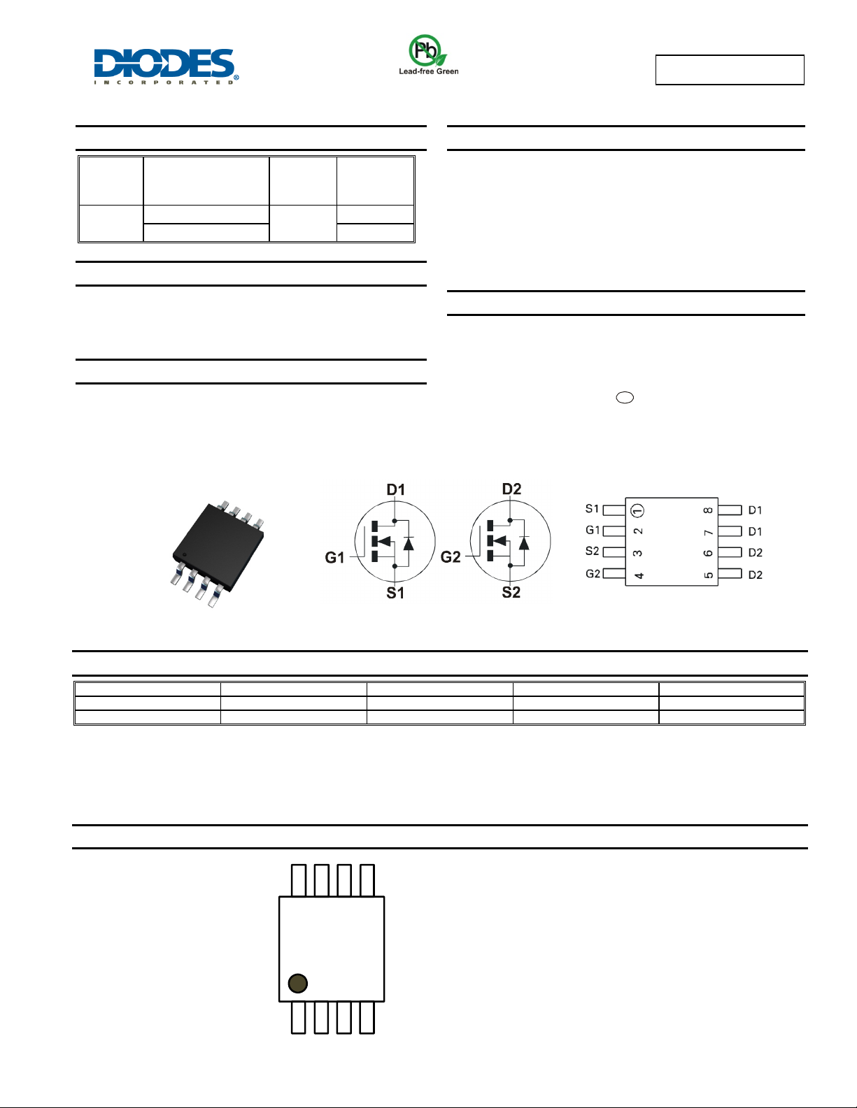
Top View
Device Symbol
Top View
Pin-Out
Ordering Information (Note 4)
Product Marking Reel size (inches) Tape width (mm) Quantity per reel
ZXMD63N03XTA ZXM63N03 7 12 1,000
ZXMD63N03XTC ZXM63N03 13 12 4,000
Notes: 1. No purposely added lead. Fully EU Directive 2002/95/EC (RoHS) & 2011/65/EU (RoHS 2) compliant.
2. See http://www.diodes.com/quality/lead_free.html for more information about Diodes Incorporated’s definitions of Halogen- and Antimony-free, "Green"
and Lead-free.
3. Halogen- and Antimony-free "Green” products are defined as those which contain <900ppm bromine, <900ppm chlorine (<1500ppm total Br + Cl) and
<1000ppm antimony compounds.
4. For packaging details, go to our website at http://www.diodes.com/products/packages.html.
Marking Information
ZXMD63N03X
Document number: DS33501 Rev. 2 - 2
ZXM6
3N03
ZXM63N03 = Product type Marking Code
1 of 8
www.diodes.com
March 2014
© Diodes Incorporated

X
ZXMD63N03
Maximum Ratings (@T
= +25°C, unless otherwise specified.)
A
Characteristic Symbol Value Unit
Drain-Source Voltage
Gate-Source Voltage
Continuous Drain Current
Steady
State
@ V
= 4.5V; T
GS
= 4.5V; T
GS
= +25°C (Note 5 & 6)
A
= +70°C (Note 5 & 6)
A
@ V
Pulsed Drain Current (Notes 6 & 7)
Continuous Source Current (Body Diode) (Notes 5 & 6)
Pulsed Source Current (Body Diode) (Notes 6 & 7)
V
DSS
V
GSS
I
D
I
DM
I
S
I
SM
30 V
±20 V
2.3
1.8
A
14 A
1.5 A
14 A
Thermal Characteristics
Characteristic Symbol Value Unit
Power Dissipation
(Notes 6 & 8)
(Notes 5 & 6) 1.25
P
D
0.87
W
(Notes 8 & 9) 1.04
143
°C/W
Thermal Resistance, Junction to Ambient
(Notes 6 & 8)
(Notes 5 & 6) 100
R
JA
(Notes 8 & 9) 120
Thermal Resistance, Junction to Leads (Note 10)
Operating and Storage Temperature Range
Notes: 5. For a device surface mounted on FR4 PCB measured at t 10 sec.
6. For device with one active die.
7. Repetitive rating - 25mm x 25mm FR4 PCB, D = 0.02, pulse width 300s – pulse width limited by maximum junction temperature.
8. For a device surface mounted on 25mm x 25mm FR4 PCB with high coverage of single sided 1oz copper, in still air conditions.
9. For device with two active die running at equal power.
10. Thermal resistance from junction to solder-point (at the end of the drain lead).
R
JL
T
, T
J
STG
84.9 °C/W
-55 to +150 °C
ZXMD63N03X
Document number: DS33501 Rev. 2 - 2
2 of 8
www.diodes.com
March 2014
© Diodes Incorporated

X
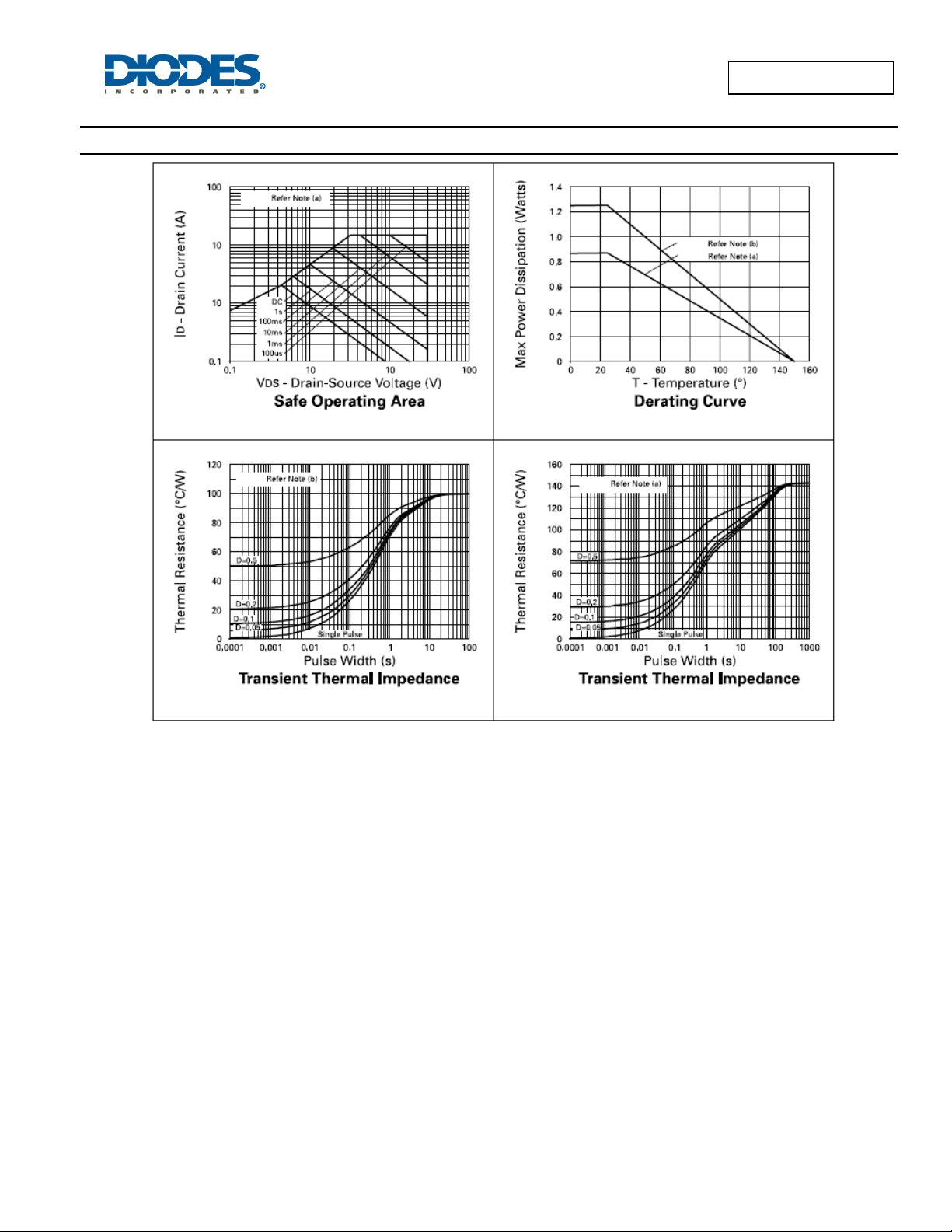
Thermal Characteristics
ZXMD63N03
ZXMD63N03X
Document number: DS33501 Rev. 2 - 2
3 of 8
www.diodes.com
March 2014
© Diodes Incorporated
 Loading...