Diodes ZXMD63C03X User Manual

ZXMD63C03X
30V DUAL N AND P-CHANNEL ENHANCEMENT MODE MOSFET
SUMMARY
N-CHANNEL: V
P-CHANNEL: V
DESCRIPTION
This new generation of high density MOSFETs from Zetex utilizes a unique
structure that combines the benefits of low on-resistance with fast switching
speed. This makes them ideal for high efficiency, low voltage, power
management applications.
FEATURES
Low on-resistance
•
Fast switching speed
•
Low threshold
•
Low gate drive
•
Low profile SOIC package
•
APPLICATIONS
•
DC - DC converters
(BR)DSS
(BR)DSS
=30V; R
=-30V; R
=0.135 ; ID=2.3A
DS(ON)
=0.185 ; ID=-2.0A
DS(ON)
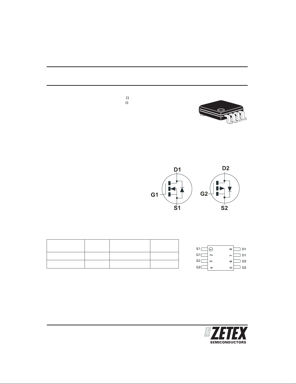
MSOP8
P-channelN-channel
•
Power management functions
•
Disconnect switches
•
Motor control
ORDERING INFORMATION
DEVICE REEL SIZE
(inches)
ZXMD63C03XTA 7 12 embossed 1,000
ZXMD63C03XTC 13 12 embossed 4,000
TAPE WIDTH
(mm)
QUANTITY
PER REEL
DEVICE MARKING
ZXM63C03
ISSUE 2 - SEPTEMBER 2007
1
Pin-out
Top view

ZXMD63C03X
ABSOLUTE MAXIMUM RATINGS
PARAMETER SYMBOL N-CHANNEL P-CHANNEL UNIT
Drain-Source Voltage V
Gate- Source Voltage V
Continuous Drain Current
(V
=4.5V; TA=25°C)(b)(d)
GS
(V
=4.5V; TA=70°C)(b)(d)
GS
Pulsed Drain Current (c)(d) I
Continuous Source Current (Body Diode)(b)(d) I
Pulsed Source Current (Body Diode)(c)(d) I
Power Dissipation at T
Linear Derating Factor
Power Dissipation at T
Linear Derating Factor
Power Dissipation at T
Linear Derating Factor
=25°C (a)(d)
A
=25°C (a)(e)
A
=25°C (b)(d)
A
Operating and Storage Temperature Range T
DSS
GS
I
D
DM
S
SM
P
D
P
D
P
D
j:Tstg
30 -30 V
⫾20 V
2.3
1.8
-2.0
-1.6
14 -9.6 A
1.5 -1.4 A
14 -9.6 A
0.87
6.9
1.04
8.3
1.25
10
-55 to +150 °C
A
A
W
mW/°C
W
mW/°C
W
mW/°C
THERMAL RESISTANCE
PARAMETER SYMBOL VALUE UNIT
Junction to Ambient (a)(d) R
Junction to Ambient (b)(d) R
Junction to Ambient (a)(e) R
NOTES:
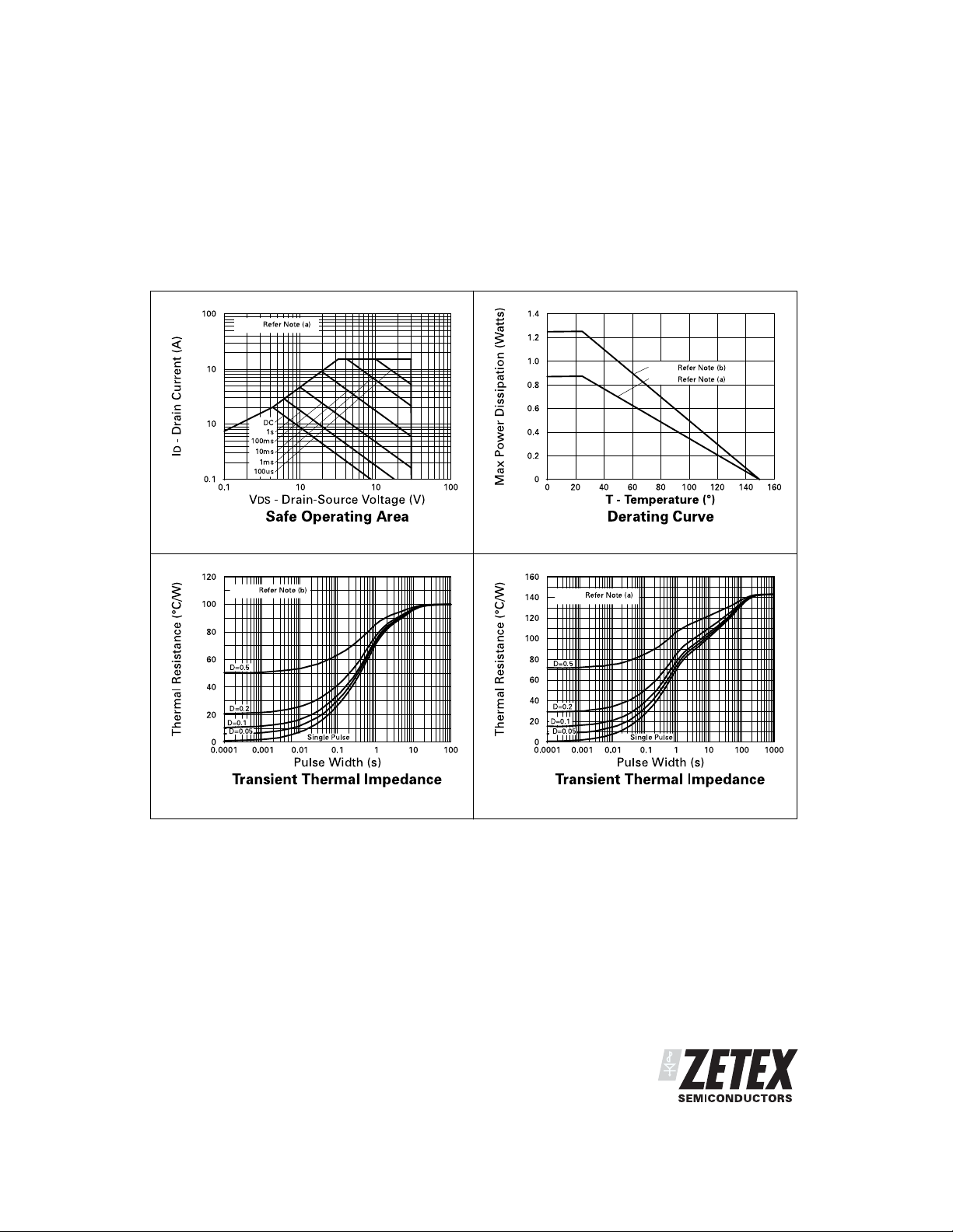
(a) For a device surface mounted on 25mm x 25mm FR4 PCB with high coverage of single sided 1oz copper, in still air conditions
(b) For a device surface mounted on FR4 PCB measured at t⭐10 secs.
(c) Repetitive rating - pulse width limited by maximum junction temperature. Refer to Transient Thermal Impedance graph.
(d) For device with one active die.
(e) For device with two active die running at equal power.
θJA
θJA
θJA
ISSUE 2 - SEPTEMBER 2007
2
143 °C/W
100 °C/W
120 °C/W

N-CHANNEL CHARACTERISTICS
ZXMD63C03X
ISSUE 2 - SEPTEMBER 2007
3

P-CHANNEL CHARACTERISTICS
ZXMD63C03X
ISSUE 2 - SEPTEMBER 2007
4
 Loading...