Diodes ZXM66P02N8 User Manual

A
f
Please click here to visit our online spice models database.
20V P-CHANNEL ENHANCEMENT MODE MOSFET
Product Summary
V
Description and Applications
This high density MOSFET utilizes a unique structure that combines
the benefits of a low on-resistance with fast switching speed. This
makes it ideal for high efficiency, low voltage power management
applications. Compared to trenchFET technology, this MOSFET
structure has an intrinsically higher pulse current handling capability
in linear mode.
• Inrush protection circuits
• DC-DC Converters
• Power management functions
• Disconnect switches
• Motor control
R
(BR)DSS
-20V
0.025Ω
SO-8
Top View
ID
DS(on)
-8.0A
Product Line o
Diodes Incorporated
ZXM66P02N8
Features and Benefits
• High pulse current handling in linear mode
• Low on-resistance
• Fast switching speed
• Low gate drive
• Low profile SOIC package
Mechanical Data
• Case: SO-8
• Case Material: Molded Plastic. UL Flammability Classification
Rating 94V-0
• Moisture Sensitivity: Level 1 per J-STD-020
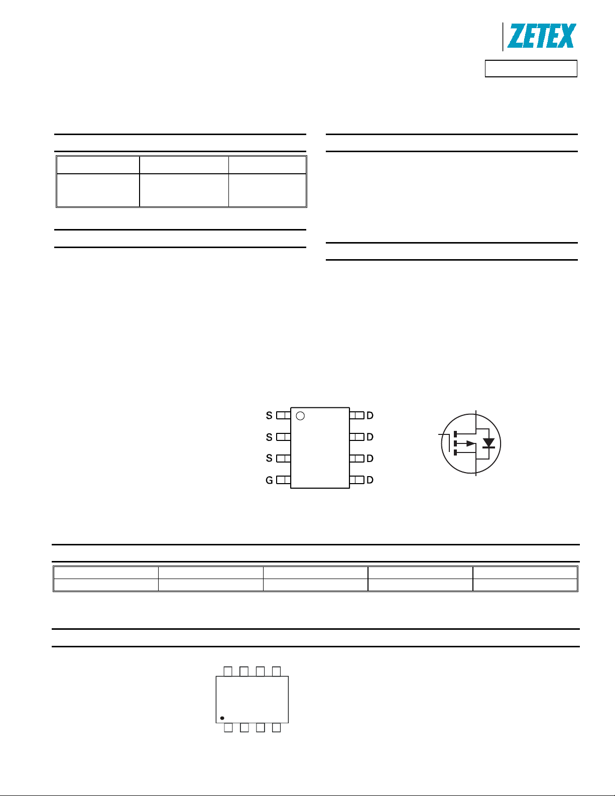
• Terminals Connections: See diagram below
• Terminals: Finish - Matte Tin annealed over Copper lead frame.
Solderable per MIL-STD-202, Method 208
• Weight: 0.074 grams (approximate)
D
G
S
Top View
Equivalent Circuit
Ordering Information (Note 1)
Product Marking Reel size (inches) Tape width (mm) Quantity per reel
ZXM66P02N8TA See below 7 12 500
Notes: 1. For packaging details, go to our website.
Marking Information
ZXM66P02N8
Document Number DS31965 Rev. 2 - 2
ZXM
66P02
YYWW
ZXM = Product Type Marking Code, Line 1
66P02 = Product Type Marking Code, Line 2
YYWW = Date Code Marking
YY = Year (ex: 09 = 2009)
WW = Week (01-52)
1 of 5
www.diodes.com
October 2009
© Diodes Incorporated

A
f
Product Line o
Diodes Incorporated
ZXM66P02N8
Maximum Ratings @T
= 25°C unless otherwise specified
A
Characteristic Symbol Value Unit
Drain-Source voltage
Gate-Source voltage
(Note 3)
Continuous Drain current
V
GS
= 4.5V
TA = 70°C (Note 3)
(Note 2)
Pulsed Drain current (Note 4)
Continuous Source current (Body diode) (Note 3)
Pulsed Source current (Body diode) (Note 4)
V
DSS
V
GS
I
D
I
DM
I
S
I
SM
-20 V
±12
-8.0
-6.5
-6.4
-28 A
-4.15 A
-28 A
Thermal Characteristics @T
= 25°C unless otherwise specified
A
Characteristic Symbol Value Unit
Power dissipation
Linear derating factor
Thermal Resistance, Junction to Ambient
Operating and storage temperature range
Notes: 2. For a device surface mounted on 25mm x 25mm FR4 PCB with high coverage of single sided 1oz copper, in still air conditions.
3. Same as note (3), except the device is measured at t ≤ 10 sec.
4. Repetitive rating 25mm x 25mm FR4 PCB, D = 0.05, pulse width 10μs – pulse width limited by maximum ju nction temperature.
(Note 2)
P
D
(Note 3)
(Note 2)
(Note 3) 50
R
JA
θ
T
, T
J
STG
1.56
12.5
2.5
20
80
-55 to 150
V
A
W
mW/°C
°C/W
°C
Electrical Characteristics @T
= 25°C unless otherwise specified
A
Characteristic Symbol Min Typ Max Unit Test Condition
OFF CHARACTERISTICS
Drain-Source Breakdown Voltage
Zero Gate Voltage Drain Current
Gate-Source Leakage
-20
BV
DSS
I
DSS
I
GSS
⎯ ⎯
⎯ ⎯
⎯ ⎯
-1
-100 nA
V
μA
ID = -250μA, V
V
= -16V, V
DS
V
= ±12V, V
GS
GS
GS
DS
= 0V
= 0V
= 0V
ON CHARACTERISTICS
Gate Threshold Voltage
Static Drain-Source On-Resistance (Note 5)
Forward Transconductance (Notes 5 & 6)
Diode Forward Voltage (Note 5)
Reverse recovery time (Note 6)
Reverse recovery charge (Note 6)
-0.7
V
GS(th)
R
⎯ ⎯
DS (ON)
g
fs
V
⎯ ⎯
SD
t
rr
Q
rr
⎯
⎯
⎯ ⎯
13.3
23.1
12.2
0.025
0.045
⎯
0.95 V
⎯
⎯
V
Ω
S
ns
nC
ID = -250μA, V
V
= -4.5V, ID = -3.2A
GS
V
= -2.5V, ID = -2.7A
GS
V
= -10V, ID = -3.2A
DS
IS = -3.2A, V
= -3.2A, di/dt = 100A/μs
I
F
GS
DS
= 0V
= VGS
DYNAMIC CHARACTERISTICS (Note 6)
Input Capacitance
Output Capacitance
Reverse Transfer Capacitance
Total Gate Charge (Note 7)
Gate-Source Charge (Note 7)
Gate-Drain Charge (Note 7)
Turn-On Delay Time (Note 7)
Turn-On Rise Time (Note 7)
Turn-Off Delay Time (Note 7)
Turn-Off Fall Time (Note 7)
Notes: 5. Measured under pulsed conditions. Pulse width ≤ 300μs; duty cycle ≤ 2%
6. For design aid only, not subject to production testing.
7. Switching characteristics are independent of operating junction temperatures.
C
⎯
iss
C
oss
C
rss
Q
⎯
g
Q
gs
Q
gd
t
⎯
D(on)
t
⎯
r
t
D(off)
t
⎯
f
⎯
⎯
⎯
⎯
⎯
2068
1038
506
43.3
3.5
21.3
14.0
44.3
118.4
98.4
⎯
⎯
⎯
⎯
⎯
⎯
⎯
⎯
⎯
⎯
pF
pF
pF
nC
nC
nC
ns
ns
ns
ns
= -15V, V
V
DS
GS
F = 1MHz
V
= -4.5V, VDS = -10V,
GS
= -3.2A
I
D
= -10V, V
V
DD
= -3.2A, RG = 6.0Ω
I
D
GS
= 0V
= -5V
ZXM66P02N8
Document Number DS31965 Rev. 2 - 2
2 of 5
www.diodes.com
October 2009
© Diodes Incorporated
 Loading...