Diodes ZXLD383 User Manual

A
Product Line o
f
Diodes Incorporated
ZXLD383
SINGLE OR MULTI CELL LED DRIVER SOLUTION
Summary
The ZXLD383 is a single or multi cell LED dri ver des ig ned for applications requiring step-up voltage conversio n from a ver y
low input voltage. The IC generates constant current pulses that are ideal for dr iving single or multiple LEDs over a wide
range of operating voltages. It includes an on/off enable input t hat can be driven directly from a photoc ell array or an open
collector/drain logic output. The enable input features an ultra-lo w voltage drop diode to ground, elim inating the need for a
photocell array isolation diode in Garden Light applications.
The ZXLD383 uses a PFM control technique to drive an internal switching transistor which exhibits a low saturation
resistance. This ensures high efficiency, even for input voltages as low as 1.0V.
The IC can start up under full load and operates down to an input voltage of below 0.9V.
The ZXLD383 is offered in the space s aving TSOT23-5 package or in die form, offering an excellent cost vs. performan ce
solution for single cell LED driving applications.
Features
• 85% Efficiency
• User adjustable output current
• Single cell operation
• Low saturation voltage
• TSOT23-3 package
• Available also in die form
• Simple application circuit
Application
• Garden lights
• Door/pathway illumination
• LED flashlight and torches
• LED backlights
• White LED driver
• Gated boost supply generator
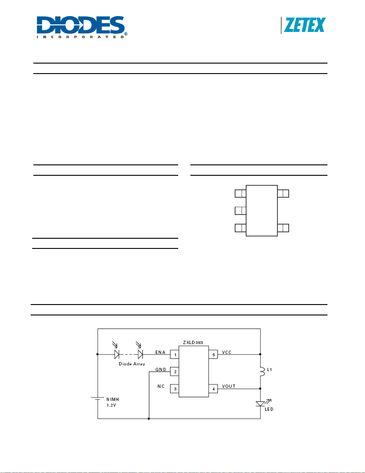
Typical Application Circuit
Pin Assignments
1
ENA
NC
2
3
GND
TSOT23-3
(Top View)
5
CC
V
4
V
OUT
ZXLD383
Document number: DS32189 Rev. 3 - 2
1 of 10
www.diodes.com
May 2010
© Diodes Incorporated

A
f
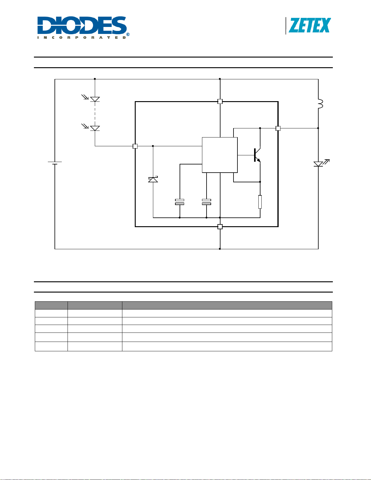
Block Diagram
Diode Array
NIMH
1.2V
ZXLD383
ENA
Dch
Fig 1. ZXLD383 Block Diagram
Product Line o
Diodes Incorporated
ZXLD383
VCC
VOUT
Pulse
Control
CoffCon
Rsense
GND
L1
LED
Pin Description
Pin No. Name Description
1 ENA Enable / Photodiode array battery charge input
2 GND Ground
3 NC Not connected (internally open circuit)
4
5
V
V
OUT
CC
ZXLD383
Document number: DS32189 Rev. 3 - 2
Switch output external inductor/LED
Supply voltage, generally Alkaline, NiMH or NiCd single cell
2 of 10
www.diodes.com
May 2010
© Diodes Incorporated

A
f
Diodes Incorporated
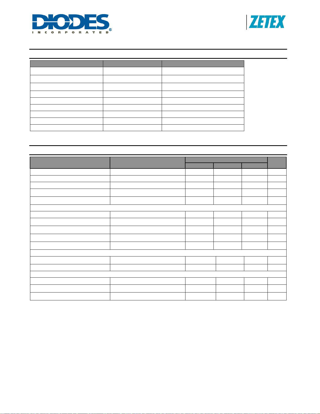
Absolute Maximum Ratings
Parameter Rating Unit
Supply Voltage (VCC)
Output Voltage (V
Enable Voltage (V
OUT
ENA
)
)
Supply Current 20 mA
Output Switch Current 800 mA
Power Dissipation (TSOT23-3) 450 mW
Power Dissipation Die 1 W
Operating Temperature Range -20 to 85 °C
Storage Temperature Range -55 to 150 °C
-0.6 to 6 V
-0.6 to 20 V
-1 to 3.5 V
Product Line o
ZXLD383
Electrical Characteristics Measured at T
Parameter Conditions
= 25°C, L = 6.8µH, I
AMB
= 0 and VCC = 1.5V unless otherwise specified.
ENA
Limits
Min Typ. Max
Units
Supply Voltage Operating Range L = 10μH 0.9 3.3 V
Minimum Supply Start-up Voltage L = 10μH 0.8 0.9 V
Supply Current Quiescent
Supply Current Shutdown
Supply Current Under-Voltage
2 4 8 mA
= VCC – 0.8V
V
ENA
VCC = 0.6V
17 30 µA
20 µA
Switch Current At turn-off 250 320 400 mA
Switch Saturation Voltage
Switch Leakage Current
Mean LED Current
Efficiency
I
OUT
V
V
V
OUT
LED
LED
= 200mA
= 20V, V
= 3.5V
= 3.5V
ENA
= 0V
100 300 mV
10 µA
40 50 65 mA
85 %
Operating Frequency
V
LED
= 3.5V
330 kHz
Discharge Pulse Width 0.7 1.5 2.5 µs
Enable Input Threshold
Enable Input Current
Enable Input Voltage
V
I
ENA
ENA
= 0.2V
= -20mA
VCC - 0.8 VCC - 0.6 VCC - 0.2
0 -11 -20 µA
0 -90 -250 mV
V
ZXLD383
Document number: DS32189 Rev. 3 - 2
3 of 10
www.diodes.com
May 2010
© Diodes Incorporated
 Loading...