

Page 1
A
Product Line o
f
Diodes Incorporated
ZXLD381
SINGLE OR MULTI CELL LED DRIVER SOLUTION
Summary
The ZXLD381 is a single cell LED driver designed for a pplications where step-up voltage conversion from a very low input
voltage is required. These applications mainly operate from 1.5V or 1.2V c ells. The IC generates constant current pulses that
are ideal for driving single or multiple LEDs over a wide range of operating voltages.
The ZXLD381 uses a PFM control technique to drive an internal switching transistor which a low saturation resistance. This
ensures high efficiency, even for input voltages as low as 1V.
The IC can start up under full load and operates down to an input voltage of only 0.9V.
The ZXLD381 is offered in the space saving SOT23 packag e or in die form, offering an excellent cost vs performance s olution
for single cell LED driving applications.
Features
• 85% Efficiency
• User adjustable output current
• Single cell operation (0.9V minimum)
• Low saturation voltage switching transistor
• SOT23-3 package
• Available also in Die form
• Simple Application circuit
Application
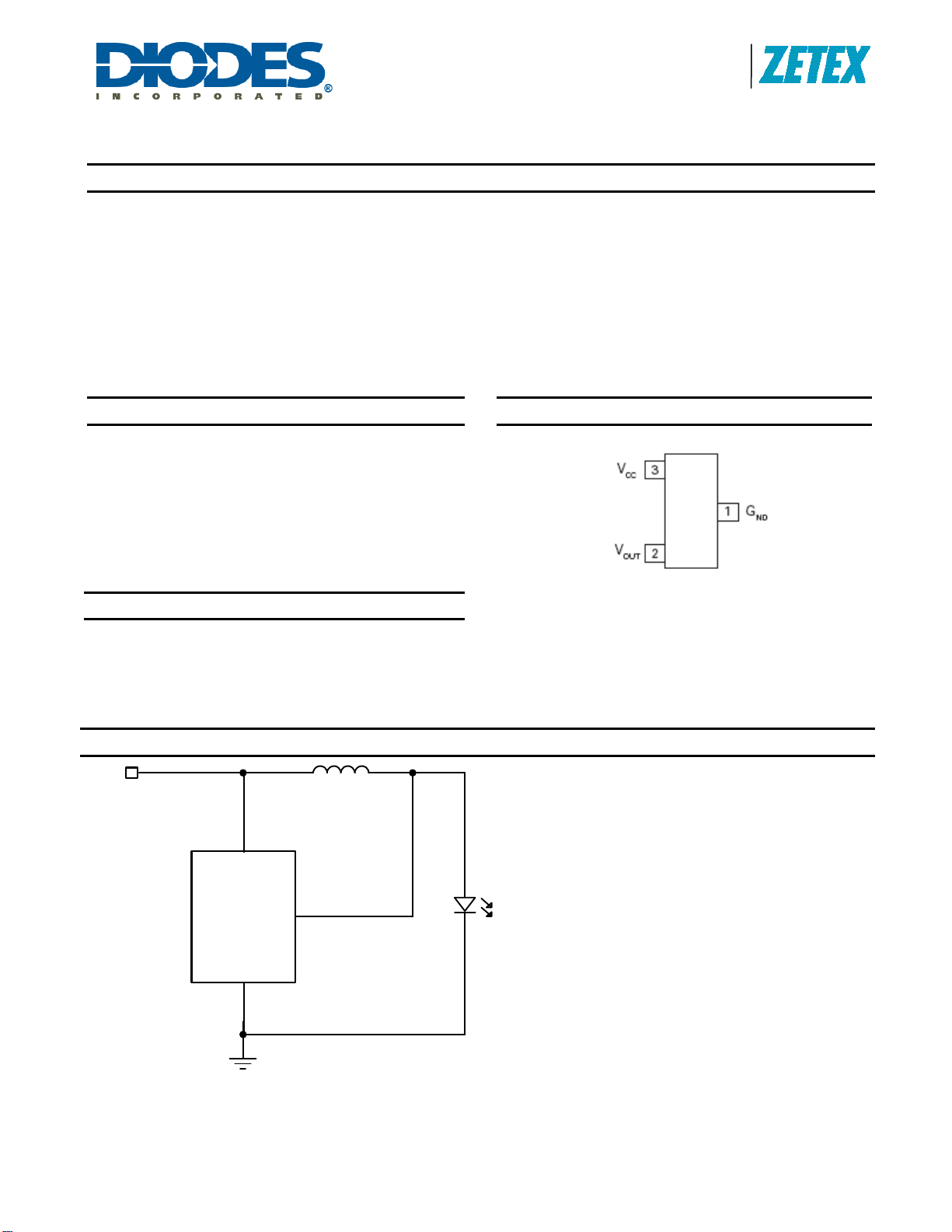
Pin Assignments
SOT23-3
(Top View)
• LED flashlights and torches
• LED backlights
• White LED driver
Typical Application Circuit
V
IN
V
CC
V
OUT
GND
ZXLD381
ZXLD381
Document number: DS32188 Rev. 3 - 2
L1
LED
1 of 9
www.diodes.com
May 2010
© Diodes Incorporated
Page 2
A
f
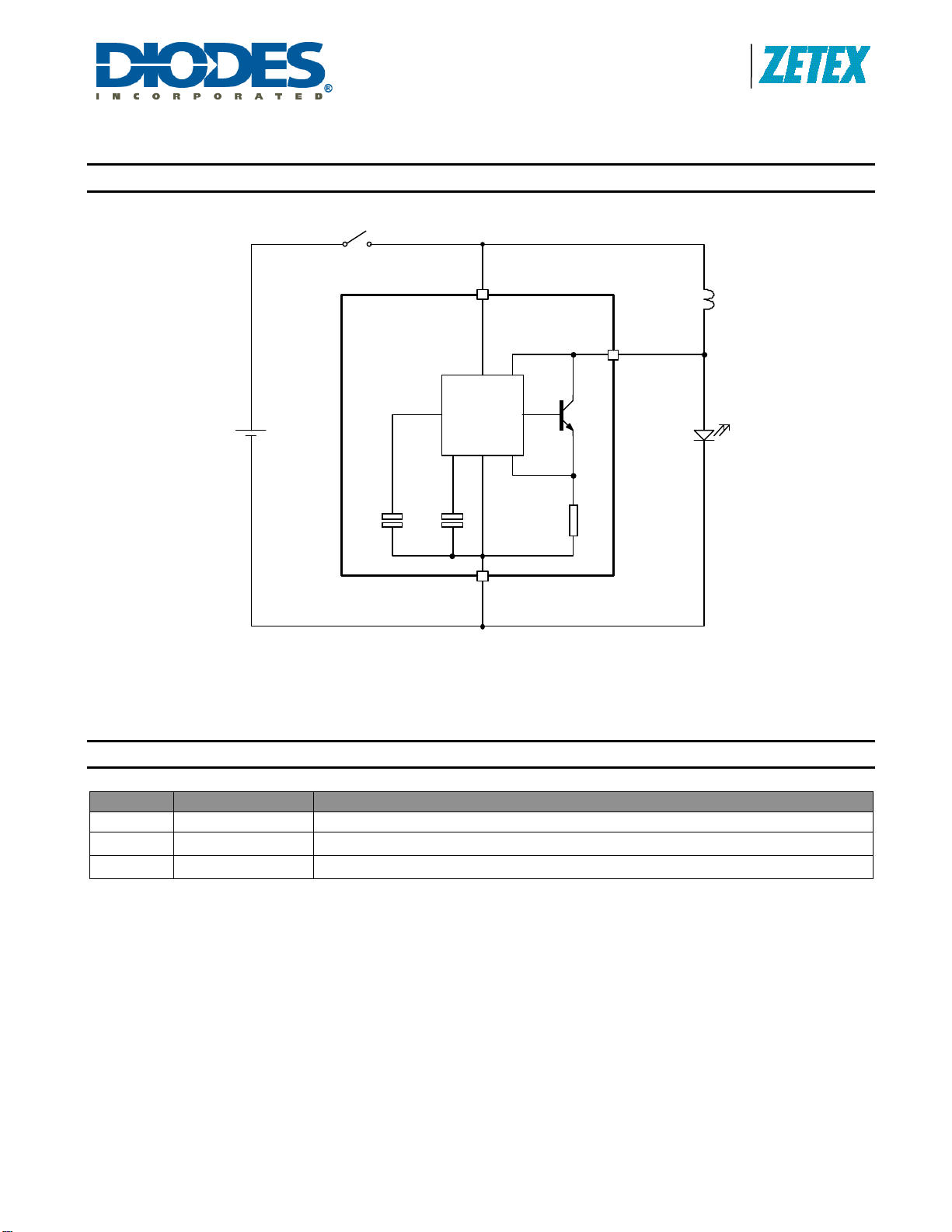
Block Diagram
1.5V
VCC
ZXLD381
Pulse
Control
Cof fCon
Rsense
GND
Fig 1. ZXLD381 Block Diagram
Product Line o
Diodes Incorporated
ZXLD381
L1
VOUT
LED
Pin Description
Pin No. Name Description
1 GND Ground
2
3
V
V
OUT
CC
ZXLD381
Document number: DS32188 Rev. 3 - 2
Switch output external inductor/LED
Supply voltage, generally Alkaline, NiMH or NiCd single cell
2 of 9
www.diodes.com
May 2010
© Diodes Incorporated
Page 3
A
f
Absolute Maximum Ratings
Parameter Rating Unit
Supply Voltage (VCC)
Output Voltage (V
Supply Current 20 mA
Output Switch Current 800 mA
Power Dissipation SOT23-3 450 mW
Power Dissipation Die 1 W
Operating Temperature Range 0 to 85 °C
Storage Temperature Range -55 to 150 °C
OUT
)
-0.6 to 10 V
-0.6 to 20 V
Product Line o
Diodes Incorporated
ZXLD381
Electrical Characteristics Measured at T
Parameter Conditions
Supply Voltage Operating Range L = 10μH 0.9 2.2 V
Minimum Supply Start-up Voltage L = 10μH 0.8 0.9 V
Switch Current At turn-off 250 320 400 mA
Switch Saturation Voltage
Switch Leakage Current
Mean LED Current
Efficiency
Operating Frequency
Discharge Pulse Width 0.7 1.5 2.5 µs
I
OUT
V
V
V
V
OUT
LED
LED
LED
= 200mA
= 25°C, L = 4.7µH and VCC = 1.5V unless otherwise specified.
AMB
Min Typ. Max
100 300 mV
= 20V
= 3.5V
= 3.5V
= 3.5V
40 70 120 µA
40 55 70 mA
85 %
350 kHz
Limits
Units
ZXLD381
Document number: DS32188 Rev. 3 - 2
3 of 9
www.diodes.com
May 2010
© Diodes Incorporated
Page 4

A
Product Line o
f
Diodes Incorporated
ZXLD381
Device Description
The ZXLD381 is a simple PFM, DC-DC controller com bined with a high performance internal switching transistor, enabling the
production of a high efficiency boost converter for use in single cell applications. A block diagr am is sho wn for the ZXLD381 in
Fig 1.
When power is applied, an oscillator within the pulse control block forces the internal switching transistor to s witch on to start
an energy charge cycle. The low saturation voltag e switch pulls the V
across the external inductor L1. This causes a current to build up, storing energ y in the inductor. During this phase, switch
current and supply voltage are monitored and use d by the pulse control circuit to determ ine the optimum drive cond itions and
on-time. At the end of the energy charge cycle, the internal switch is turne d off rapidly, in terrupting the current fl ow through L1
which causes the voltage on V
voltage, the inductor current is transferred from the internal switch to the LED, starting the energ y discharge cycle. With the
voltage across the inductor reversed, the current flowing through it (and the LED) no w falls. When the inductor current reach e s
zero, the voltage on the V
next energy charge cycle. Except for low level losses, all the energy stored in the inductor during a charge cycle will be
channeled to the load LED during the following discharge cycle.
The current fed into the load LED has a sawtooth waveform, the average (DC) value of which is kept constant by the pulse
control circuit for varying supply voltage and temperature. It is possible to change the output current given by the ZXLD38 1 by
changing the value of inductor L1. The larger the inductance of L1, the lower the output current. A table/graph showing the
relationship between inductance and output current is given later in this datasheet. Since the output current of the ZXLD3 81 is
a sawtooth waveform, its peak value is substantially larger than the DC/average value. The table also provid es this data.
The internal switching transistor has a minimum collector-emitter breakd own voltage of 20V and this sets the maximum load
voltage allowable. The minimum value is set by a f eature of the pulse control circuit that requires the load voltage to be at least
0.8V greater than V
impaired.) Higher than nominal load voltages will lower the average (DC) output current generated for a given inductor value.
OUT
. (The device will function with load voltages smaller than this but output current regulation will be
CC
to rise dramatically. When the voltage on V
OUT
pin falls back towards VCC. This action is sensed by the pulse control circuit, which initiates the
pin close to ground which forces the supply voltage
OUT
reaches the load LED's forward (on)
OUT
ZXLD381
Document number: DS32188 Rev. 3 - 2
4 of 9
www.diodes.com
May 2010
© Diodes Incorporated
Page 5

A
f
Typical Characteristics
100
90
80
70
2.2µH
3.3µH
100
90
80
70
Product Line o
Diodes Incorporated
22µH
47µH
15µH
10µH
ZXLD381
OUT
I (mA)
350
300
250
200
IN
I (mA)
150
60
50
40
30
20
10
0
0.8
11.2
I vs. V for L = 2.2µH to 47µH
OUT(AVERA GE) CC
2.2µH
3.3µH
6.8µH
4.7µH
1.4 1.6
V (V)
CC
4.7µH
10µH
47µH
1.8
6.8µH
15µH
22µH
60
50
6.8µH
40
Efficiency (%)
4.7µH
30
20
3.3µH
10
2.2µH
0
2
0.8 1 1.2 1.4 1.6 1.8 2
V (V)
Efficiency vs. V for L = 2.2µH to 47µH
CC
CC
10µH
100
15µH
22µH
50
47µH
0
0.8 1 1.2 1.4 1.6 1.8 2
I vs. V for L = 2.2µH to 47µH
IN CC
V (V)
CC
Channel-1 (Upper): I @ 100mA/cm
Channel-2 (Low er): V @ 1V/cm
LED
OUT
Timebase: 500ns/cm
Operating Waveforms for L = 4.7µH, V = 1.5V
CC
Notes: V
= 3.5V for all graphs
LED
ZXLD381
Document number: DS32188 Rev. 3 - 2
5 of 9
www.diodes.com
May 2010
© Diodes Incorporated
Page 6

A
f
Typical Characteristics (Cont.)
450
400
350
300
250
200
OSC
f (kHz)
150
100
50
Product Line o
Diodes Incorporated
ZXLD381
0
0.8 1 1.2 1.4 1.6 1.8 2
f vs. V for L = 47µH
OSC CC
V (V)
CC
Notes: V
= 3.5V for all graphs
LED
ZXLD381
Document number: DS32188 Rev. 3 - 2
6 of 9
www.diodes.com
May 2010
© Diodes Incorporated
Page 7

A
f
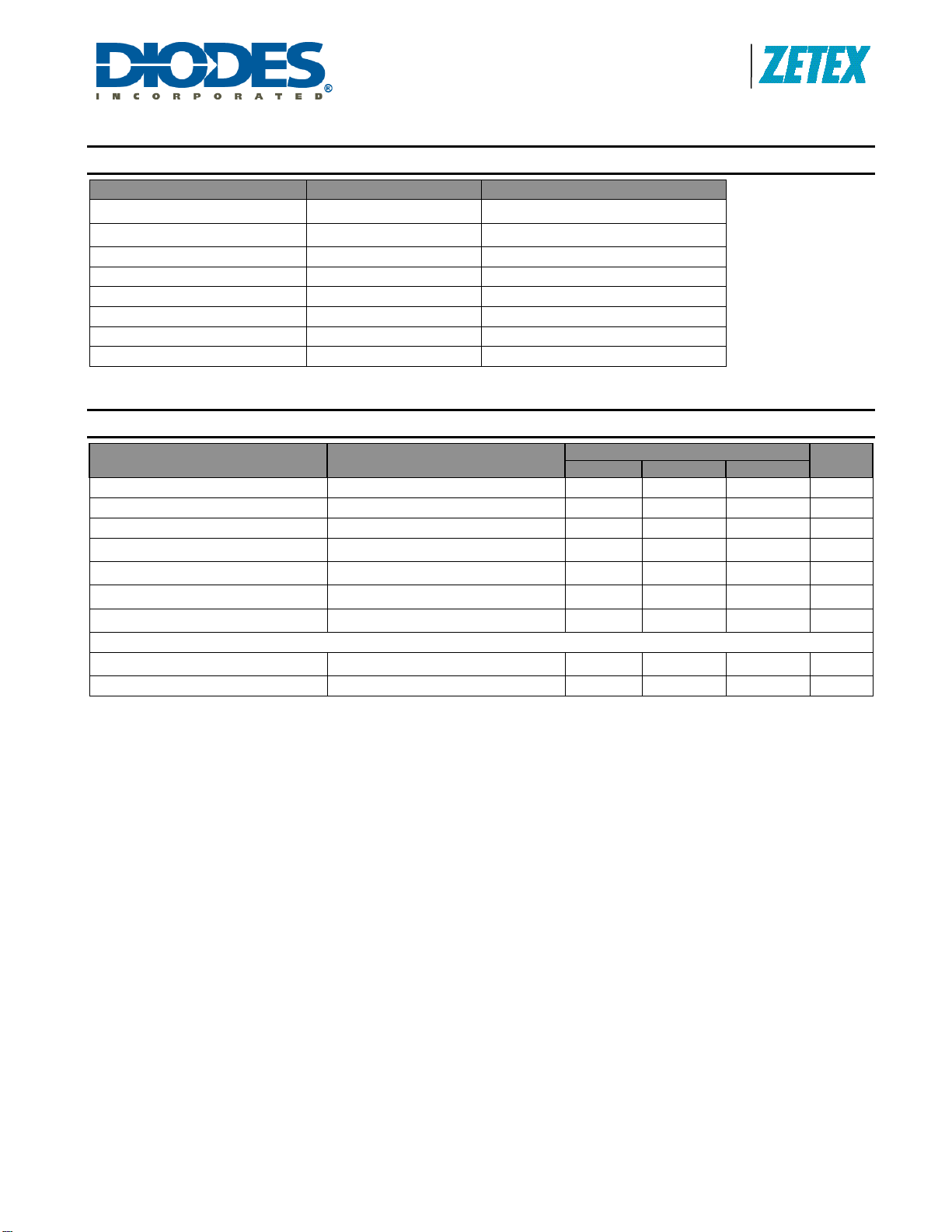
Application Examples
Standard Operating Mode
Notes: V
Low Ripple LED Current Mode
Notes: V
= 3.5V
LED
= 3.5V, D1 = ZHCS1000, C1 = 1F (low ESR)
LED
Product Line o
Diodes Incorporated
ZXLD381
ZXLD381
Document number: DS32188 Rev. 3 - 2
7 of 9
www.diodes.com
May 2010
© Diodes Incorporated
Page 8

A
Product Line o
f
Diodes Incorporated
ZXLD381
Ordering Information
Part Number Package Part Mark
ZXLD381FHTA SOT23 381 8 3000
Tape Width
(mm)
Quantity
(per reel)
Package Outline Dimensions
b
3leads
L1
Dim.
A - 1.12 - 0.044 e1 1.90 NOM 0.075 NOM
A1 0.01 0.10 0.0004 0.004 E 2.10 2.64 0.083 0.104
b 0.30 0.50 0.012 0.020 E1 1.20 1.40 0.047 0.055
c 0.085 0.20 0.003 0.008 L 0.25 0.60 0.0098 0.0236
D 2.80 3.04 0.110 0.120 L1 0.45 0.62 0.018 0.024
e 0.95 NOM 0.037 NOM - - - - -
ZXLD381
Document number: DS32188 Rev. 3 - 2
E
e
e1
E1
D
A
A1
Millimeters Inches
Min. Max. Min. Max. Min. Max. Min. Max.
L
c
Millimeters Inches
Dim.
8 of 9
www.diodes.com
May 2010
© Diodes Incorporated
Page 9

A
Product Line o
f
Diodes Incorporated
ZXLD381
DIODES INCORPORATED MAKES NO WARRANTY OF ANY KIND, EXPRESS OR IMPLIED, WITH REGARDS TO THIS DOCUMENT,
INCLUDING, BUT NOT LIMITED TO, THE IMPLIED WARRANTIES OF MERCHANTABILITY AND FITNESS FOR A PARTICULAR PURPOSE
(AND THEIR EQUIVALENTS UNDER THE LAWS OF ANY JURISDICTION).
Diodes Incorporated and its subsidiaries reserve the right to make modifications, enhancements, improvements, corrections or other changes
without further notice to this document and any product described herein. Diodes Incorporated does not assume any liability arising out of the
application or use of this document or any product described herein; neither does Diodes Incorporated convey any license under its patent or
trademark rights, nor the rights of others. Any Customer or user of this document or products described herein in such applications shall assume
all risks of such use and will agree to hold Diodes Incorporated and all the companies whose products are represented on Diodes Incorporated
website, harmless against all damages.
Diodes Incorporated does not warrant or accept any liability whatsoever in respect of any products purchased through unauthorized sales channel.
Should Customers purchase or use Diodes Incorporated products for any unintended or unauthorize d application, Customers shall indemnify and
hold Diodes Incorporated and its representatives harmless against all claims, damages, expenses, and attorney fees arising out of, directly or
indirectly, any claim of personal injury or death associated with such unintended or unauthorized application.
Products described herein may be covered by one or more United States, international or foreign patents pending. Product names and markings
noted herein may also be covered by one or more United States, international or foreign trademarks.
Diodes Incorporated products are specifically not authorized for use as critical components in life support devices or systems without the express
written approval of the Chief Executive Officer of Diodes Incorporated. As used herein:
A. Life support devices or systems are devices or systems which:
1. are intended to implant into the body, or
2. support or sustain life and whose failure to perform when properly used in accordance with instructions for use provided in the
labeling can be reasonably expected to result in significant injury to the user.
B. A critical component is any component in a life support device or system whose failure to perform can be reasonably expected to cause the
failure of the life support device or to affect its safety or effectiveness.
Customers represent that they have all necessary expertise in the safety and regulatory ramifications of their life support devices or systems, and
acknowledge and agree that they are solely responsible for all legal, regulatory and safety-related requirements concerning their products and any
use of Diodes Incorporated products in such safety-critical, life support devices or systems, notwithstanding any devices- or systems-related
information or support that may be provided by Diodes Incorporated. Further, Customers must fully indemnify Diodes Incorporated and its
representatives against any damages arising out of the use of Diodes Incorporated products in such safety-critical, life support devices or systems.
Copyright © 2010, Diodes Incorporated
www.diodes.com
IMPORTANT NOTICE
LIFE SUPPORT
ZXLD381
Document number: DS32188 Rev. 3 - 2
9 of 9
www.diodes.com
May 2010
© Diodes Incorporated
 Loading...