

Page 1
ZXLD1615
ADJUSTABLE DC-DC BOOST CONVERTER WITH INTERNAL SWITCH IN
TSOT23-5
DESCRIPTION
The ZXLD1615 is a PFM inductive boost converter
designed to provide output voltages of up to 28V
from a 2.5V to 5.5V input supply.
The ZXLD1615 includes the output switch and peak
current sense resistor, and can provide up to 10mA
output current at maximum output voltage. Higher
current is available at lower output voltages.
Quiescent current is typically 60A and a shutdown
function is provided to reduce this current to less
than 100nA in the 'off' state.
ADVANCED FEATURES
Internal 30V NDMOS switch
•
True analog output voltage control via PWM
•
with internal filter
FEATURES
Low profile TSOT23-5 pin package
•
•
Internal PWM filter for adjustable output
•
High efficiency (85% typ)
•
Wide input voltage range: 2.5V to 5.5V
•
Up to 250mA output current at 5V
Nominal output voltage can be set up to a maximum
of 28V by two external resistors and can be adjusted
to lower values by a PWM control signal applied to
the 'Enable' pin. Depending upon the control
frequency, the PWM signal will provide either
continuous (low ripple) or gated control. The PWM
filter components are contained within the chip.
Minimum output voltage is determined by the input
supply.
The device is assembled in a low profile TSOT23-5
pin package.
APPLICATIONS
LCD and OLED bias
•
Cellular / mobile phones
•
Digital cameras
•
• PDAs
•
LCD modules
•
Varactor and PIN diode bias
•
Palmtop computers
•
Low quiescent current: (60A typ)
•
100nA maximum shutdown current
•
Up to 1MHz switching frequency
•
Low external component count
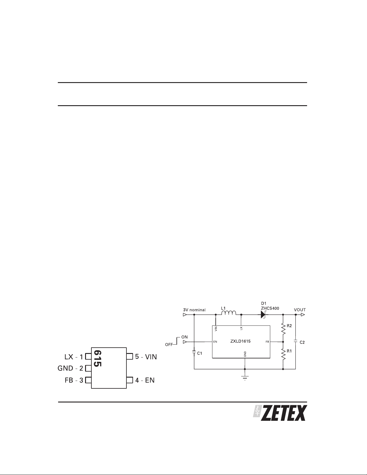
PINOUT
TOP VIEW
ISSUE 3 - AUGUST 2004
TYPICAL APPLICATION CIRCUIT
1
SEMICONDUCTORS
Page 2
ZXLD1615
ABSOLUTE MAXIMUM RATINGS
(Voltages to GND unless otherwise stated)
Input voltage (V
LX output voltage (V
Switch output current (I
Power dissipation (PD) 300mW
Operating temperature (T
Storage temperature (T
Junction temperature (Tj
ELECTRICAL CHARACTERISTICS: (Test conditions: V
Symbol Parameter Conditions Min Typ Max Units
V
IN
I
IN
V
FB
f
LX
T
OFF
(2)
T
ON
I
LXpk
R
LX
I
LX(leak)
V
ENH
V
ENL
I
ENL
I
ENH
(3)
T
EN(hold)
⌬T/T PWM duty cycle range at
f
LPF
A
LPF
)7V
IN
) 30V
LX
) 500mA
LX
) -40 to 85°C
OP
) -55 to 150°C
ST
) 125°C
MAX
IN=VEN
=3V, T
=25°C unless otherwise stated
AMB
(1)
Input voltage 2.5 5.5 V
Supply current
60
<10
100
100µAnA
Quiescent
Shutdown
V
EN=VIN,ILX
=0V
V
EN
= 0,Output not switching
FB pin control voltage 0.98 1.07 V
Operating frequency L=10H, V
=28V, 5mA load 600 kHz
OUT
LX output ‘OFF’ time 350 500 ns
LX output ‘ON’ time 5µs
Switch peak current limit L=10H, V
=28V, 5mA load 320 mA
OUT
Switch 'On' resistance 1.75 ⍀
Switch leakage current VLX=20V 1 µA
EN pin high level Input voltage Device active 1.5 V
IN
EN pin low level Input voltage Device in shutdown 0.4 V
EN pin low level input current VEN=0V -100 nA
EN pin high level input current VEN=V
IN
1 A
EN pin turn off delay VENswitched from high to low 120 µs
‘EN’ input for dc output
10kHz<f<100kHz, V
ENH=VIN
20 100 %
voltage control
Internal PWM low pass filter
4 kHz
cut-off frequency
Filter attenuation f=30kHz 52.5 dB
)
V
NOTES:
1 Production testing of the device is performed at 25°C. Functional operation of the device over a –40°C to +85°C temperature range is
guaranteed by design, characterization and process control.
2 Nominal ‘on’ time (TONnom ) is defined by the input voltage (V
T
= {I
ONnom
3 This is the time for which the device remains active after the EN pin has been asserted low. This delay is necessary to allow the output to be
maintained during dc PWM mode operation.
4 The maximum PWM signal frequency during this mode of operation should be kept as low as possible to minimize errors due to the turn-off
delay
LX(pkdc)
x L/VIN} +200ns
), coil inductance (L) and peak current (I
IN
) according to the expression:
LXpkdc
ISSUE 3 - AUGUST 2004
SEMICONDUCTORS
2
Page 3
PIN DESCRIPTION
Pin No. Name Description
LX Output of NDMOS switch
1
GND Ground (0V)
2
FB Feedback pin for voltage control loop
3
Nominal voltage 1.025V
EN Enable input (active high to turn on device)
4
Also used to adjust output current by PWM signal.
Connect to V
V
5
IN
Input voltage (2.5V to 5.5V). Decouple with capacitor close to device.
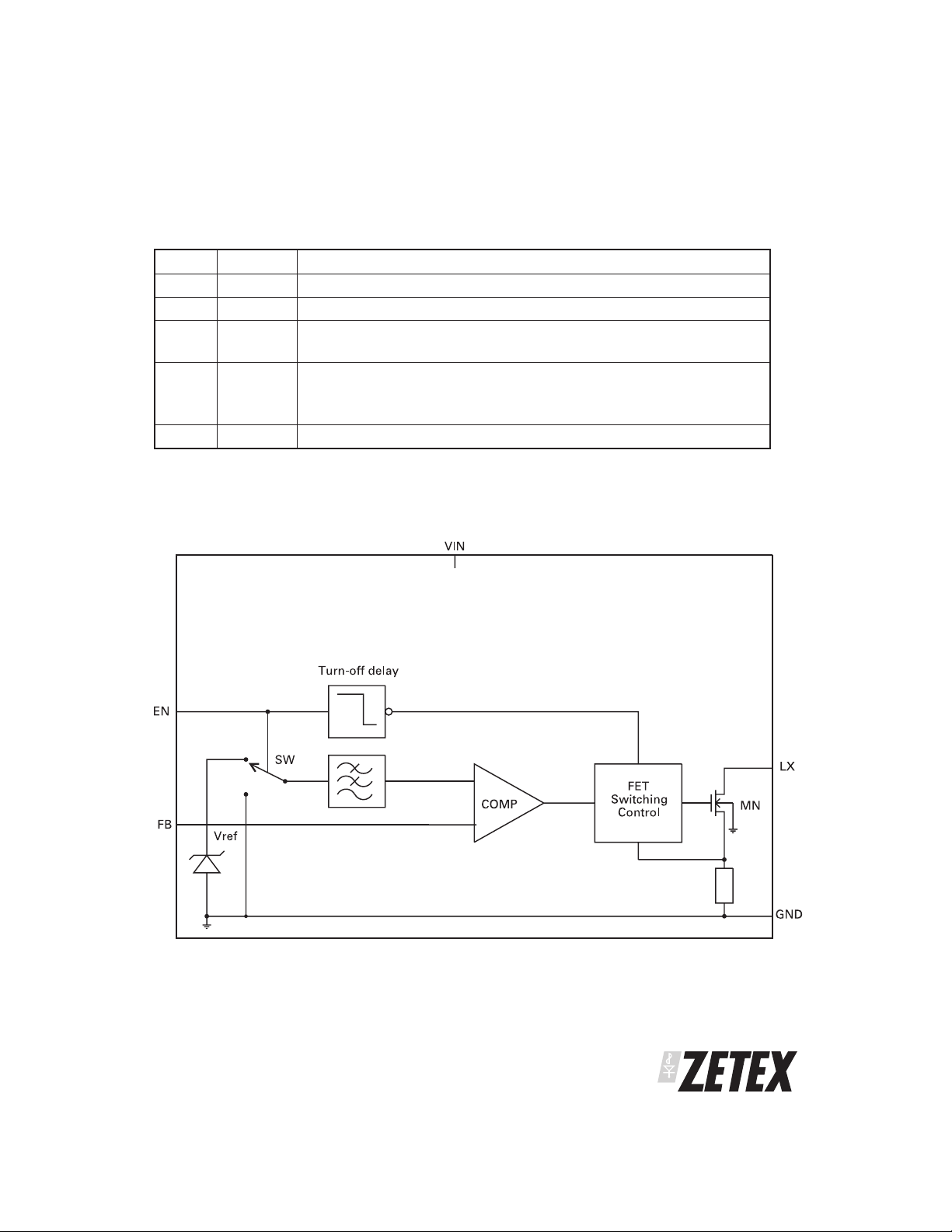
BLOCK DIAGRAM
for permanent operation.
in
ZXLD1615
ISSUE 3 - AUGUST 2004
3
SEMICONDUCTORS
Page 4

ZXLD1615
Device Description
The device is a PFM flyback dc-dc boost converter,
working in discontinuous mode.
With reference to the chip block diagram and typical
application circuit, the operation of the device is as
follows:
Control loop
When 'EN' is high, the control circuits become active
and the low side of the coil (L1) is switched to ground
via NDMOS transistor (MN). The current in L1 is
allowed to build up to an internally defined level
(nominally 320mA) before MN is turned off. The
energy stored in L1 is then transferred to the output
capacitor (C2) via schottky diode (D1). The output
voltage is sensed at pin 'FB' by external resistors R1
and R2 and compared to a reference voltage V
(1.025V nominal). A comparator senses when the
output voltage is above that set by the reference and
its output is used to control the 'off' time of the
output switch. The control loop is self-oscillating,
producing pulses of up to 5s maximum duration
(switch 'on'), at a frequency that varies in proportion
to the output current. The feedback loop maintains a
voltage of V
maximum output voltage equal to V
The minimum 'off' time of the output switch is fixed
at 0.5s nominal, to allow time for the coil's energy
to be dissipated before the switch is turned on again.
This maintains stable and efficient operation in
discontinuous mode.
at the FB pin and therefore defines a
REF
REF
REF
*(R1+R2)/R1.
Filtered PWM operation
The input of an internal low pass filter is switched to
V
when the EN pin is high and switched to ground
REF
when the EN pin is low. The output of this filter
drives the comparator within the control loop. A
continuous high state on EN therefore provides a
filtered voltage of value Vref to the comparator.
However, by varying the duty cycle of the EN signal
at a suitably high frequency (f>10kHz), the control
loop will see a voltage, that has an average value
equal to the duty cycle multiplied by V
provides a means of adjusting the output voltage to a
lower value. It also allows the device to be both
turned on and adjusted with a single signal at the
‘EN’ pin. The output during this mode of operation
will be a dc voltage equal to V
cycle.
*(R1+R2)/R1 x duty
REF
REF
. This
Gated PWM operation
The internal circuitry of the ZXLD1615 is turned off
when no signal is present on the 'EN' pin for more
than 120s (nominal). A low frequency signal applied
to the EN pin will therefore gate the device 'on' and
'off' at the gating frequency and the duty cycle of this
signal can be varied to provide an average output
equal to V
accuracy, the gating frequency should be made as
low as possible (e.g. below 1kHz), such that the turn
off delay of the chip is only a small proportion of the
gating period
Further details of setting output current are given in
the application notes.
*(R1+R2)/R1 x duty cycle. For best
REF
SEMICONDUCTORS
ISSUE 3 - AUGUST 2004
4
Page 5

TYPICAL CHARACTERISTICS
ZXLD1615
ISSUE 3 - AUGUST 2004
5
SEMICONDUCTORS
Page 6

ZXLD1615
TYPICAL PERFORMANCE GRAPHS
(For typical applications circuit at 22H Murata LQH32CN series, TA=25 °C unless otherwise stated)
SEMICONDUCTORS
ISSUE 3 - AUGUST 2004
6
Page 7

APPLICATIONS
Setting output voltage
The ZXLD1615 has an adjustable output voltage
allowing the end user maximum flexibility. To set the
output voltage a potential divider network is needed
(see R1 and R2 in typical applications circuit).
The output voltage is determined by the equation:
R
2
⎛
⎞
⎜
VV
=+
OUT FB
where VFB = 1.025V.
The following table gives suggested values for
various output voltages.
Required
output voltage
5V 270K⍀ 1M⍀
12V 91K⍀ 1M⍀
18V 60K⍀ 1M⍀
21V 51K⍀ 1M⍀
25V 43K⍀ 1M⍀
28V 39K⍀ 1M⍀
Output voltage can be adjusted from V
maximum output voltage rating of the internal
switch, 30V.
Once the nominal output voltage has been set, it can
be adjusted to a lower value by applying a pulse
width modulated (PWM) control signal to the EN pin.
PWM adjustment permits the device to be turned on
and the output voltage set by a single logic signal
applied to the EN pin. No external resistors are
required and the amplitude of the control signal is
not critical, providing it conforms to the limits
defined in the electrical characteristics.
⎟
1
⎝
⎠
R
1
R1 R2
+ VFto the
IN
ZXLD1615
1) PWM output voltage adjustment (analogue mode)
During this mode of operation the device operation is
continuous, providing a low ripple output voltage
(V
) directly proportional to the duty cycle (D) of
OUT
the logic signal applied to the EN pin according to the
relationship:
V
= D x V
OUT
Square wave signals applied to the EN pin, for
example, will turn the device on and produce a
nominal regulated output of 13.5V.
The ZXLD1615 contains a timing circuit that switches
the device on a few microseconds after the
application of a rising edge to EN and turns it back
off again nominally 120µs after the falling edge of
EN. For continuous PWM mode operation, the
frequency of the control signal must therefore be
maintained above 10kHz at all times, to prevent the
internal delay circuit from timing out and switching
the device into standby mode. The maximum
frequency applied to EN should be limited to 100kHz
to minimize errors due to internal switching delays
2) PWM output voltage adjustment (gated mode)
This method of adjustment can be used in
applications where the output ripple is less important
than the supply current. The method of adjustment is
the same as in 1) above, however, during this mode
of operation, the device is gated on and off,
providing an average output voltage (V
proportional to the duty cycle (D) of the logic signal
applied to the EN pin according to the relationship:
V
OUT(AVG)
The ripple on this voltage will be determined by the
size of the output capacitor.
The output voltage can be adjusted all the way down
to the input voltage by either method of PWM
control, but for best results, the duty cycle range
should be kept within the specified range. Lower duty
cycles will result in increased output ripple and
non-linearity in the relationship between duty cycle
and output voltage. If a greater control range is
required, the nominal output can be reduced by the
use of external resistors before the PWM signal is
applied.
OUT(nom)
= D x V
OUT(nom)
OUT
) directly
ISSUE 3 - AUGUST 2004
Minimizing output voltage ripple
For applications requiring lower output ripple it may
be necessary to add a small ceramic capacitor in
parallel with R2. A value of 4.7pF is suitable for most
output ranges.
7
SEMICONDUCTORS
Page 8

ZXLD1615
Capacitor selection
A ceramic capacitor grounded close to the GND pin
of the package is recommended at the output of the
device. Surface mount types offer the best
performance due to their lower inductance. A
minimum value of 0.22F is advised, although higher
values will lower switching frequency and improve
efficiency especially at lower load currents. A higher
value will also minimize ripple when using the device
to provide an adjustable dc output current.
A good quality, low ESR capacitor should also be
used for input decoupling, as the ESR of this
capacitor is effectively in series with the source
impedance and lowers overall efficiency. This
capacitor has to supply the relatively high peak
current to the coil and smooth the current ripple on
the input supply. A minimum value of 4.7F is
acceptable if the input source is close to the device,
but higher values will improve performance at lower
input voltages, when the source impedance is high.
The input capacitor should be mounted as close as
possible to the IC.
Inductor selection
The choice of inductor will depend on available
board space as well as required performance. Small
value inductors have the advantage of smaller
physical size and may offer lower series resistance
and higher saturation current compared to larger
values. A disadvantage of lower inductor values is
that they result in higher frequency switching, which
in turn causes reduced efficiency due to switch
losses. Higher inductor values can provide better
performance at lower supply voltages. However, if
the inductance is too high, the output power will be
limited by the internal oscillator, which will prevent
the coil current from reaching its peak value. This
condition will arise whenever the ramp time (I
x L/VIN) exceeds the nominal 5s maximum 'on' time
limit for the LX output.
LX(peak)
For maximum stability over temperature, capacitors
with X7R dielectric are recommended, as these have
a much smaller temperature coefficient than other
types.
A table of recommended manufacturers is provided
below:
Manufacturer Website
Murata www.murata.com
Taiyo Yuden www.t-yuden.com
Kemet www.kement.com
AVX www.avxcorp.com
Recommended inductor values for the ZXLD1615 are
in the range 6.8H to 22H. The inductor should be
mounted as close to the device as possible with low
resistance connections to the LX and V
Suitable coils for use with the ZXLD1615 are shown
in the table below:
IN
pins.
Part No. L
(
CMD4D11-100MC 10 0.457 0.5 Sumid a
DO1608-103 10 0.16 1.1 Coilcraft
LQH31CN100 10 1.3 0.23 Murata
LB2012Y100MR 10 0.5 0.1 Taiyo Yuden
SEMICONDUCTORS
DCR
H)
( )
I
Manufacturer
SAT
(A)
www.sumida.com
www.coilcraft.com
www.murata.com
www.t-yuden.com
8
ISSUE 3 - AUGUST 2004
Page 9

Diode selection
The rectifier diode (D1) should be a fast low
capacitance schottky diode with low reverse leakage
at the working voltage. It should also have a peak
current rating above the peak coil current and a
continuous current rating higher than the maximum
output load current.
The table below gives some typical characteristics for
diodes that can be used with the ZXLD1615:
ZXLD1615
Diode VF@ 100mA (mV) I
ZHCS400 300 1000 400 15 SOD323
ZHCS500 300 1000 500 15 SOT23
Layout considerations
PCB tracks should be kept as short as possible to
minimize ground bounce, and the ground pin of the
device should be soldered directly to the ground
plane. It is particularly important to mount the coil
and the input/output capacitors close to the device to
minimize parasitic resistance and inductance, which
will degrade efficiency. The FB pin is a high
impedance input, so PCB track lengths to this should
also be kept as short as possible to reduce noise
pickup. Excess capacitance from the FB pin to ground
should be avoided.
(mA) Ic (mA) IRat 30V ( A) Package
FSM
ISSUE 3 - AUGUST 2004
9
SEMICONDUCTORS
Page 10

ZXLD1615
REFERENCE DESIGNS
General Boost Converter
VIN=2.5V to 5.5V, V
See page 7 in datasheet for R1 and R2 values for various output voltages.
OUT
up to 28V
1 Cell Li-Ion to 3.3V Sepic Converter
SEMICONDUCTORS
ISSUE 3 - AUGUST 2004
10
Page 11

1 Cell Li-Ion to 5V Sepic Converter
Triple Output Boost Converter for LCD or OLED Bias
ZXLD1615
Note: For all manufacturers listing please refer to application section on page 7 of this datasheet.
ISSUE 3 - AUGUST 2004
11
SEMICONDUCTORS
Page 12

ZXLD1615
PACKAGE OUTLINE
PACKAGE DIMENSIONS
Millimeters Inches
DIM
MIN. MAX. MIN. MAX.
A - 1.00 - 0.0393
A1 0.01 0.10 0.0003 0.0039
A2 0.84 0.90 0.0330 0.0354
b 0.30 0.45 0.0118 0.0177
c 0.12 0.20 0.0047 0.0078
D 2.90 BSC 0.114 BSC
E 2.80 BSC 0.110 BSC
E1 1.60 BSC 0.062 BSC
e 0.95 BSC 0.037 BSC
e1 1.90 BSC 0.074 BSC
L 0.30 0.50 0.0118 0.0196
L2 0.25 BSC 0.010 BSC
Q 4° 12° 4° 12°
ORDERING INFORMATION
DEVICE DEVICE DESCRIPTION TEMPERATURE
RANGE
ZXLD1615ET5 Boost converter in SOT23-5 -40°C to +85°C 615 TA, TC
PART MARK TAPING OPTIONS
TA reels 3,000 devices, TC reels 10,000 devices
© Zetex Semiconductors plc 2004
Europe
Zetex GmbH
Streitfeldstraße 19
D-81673 München
Germany
Telefon: (49) 89 45 49 49 0
Fax: (49) 89 45 49 49 49
europe.sales@zetex.com
These offices are supported by agents and distributors in major countries world-wide.
Thispublicationisissued to provideoutlineinformationonly which(unless agreed by the Companyin writing)may not be used, appliedor reproduced
for any purpose or form part of any order or contract or be regarded as a representation relating to the products or services concerned. The Company
reserves the right to alter without notice the specification, design, price or conditions of supply of any product or service.
For the latest product information, log on to www.zetex.com
Americas
Zetex Inc
700 Veterans Memorial Hwy
Hauppauge, NY 11788
USA
Telephone: (1) 631 360 2222
Fax: (1) 631 360 8222
usa.sales@zetex.com
Asia Pacific
Zetex (Asia) Ltd
3701-04 Metroplaza Tower 1
Hing Fong Road, Kwai Fong
Hong Kong
Telephone: (852) 26100 611
Fax: (852) 24250 494
asia.sales@zetex.com
Corporate Headquarters
Zetex Semiconductors plc
Lansdowne Road, Chadderton
Oldham, OL9 9TY
United Kingdom
Telephone (44) 161 622 4444
Fax: (44) 161 622 4446
hq@zetex.com
ISSUE 3 - AUGUST 2004
SEMICONDUCTORS
12
 Loading...