Diodes ZXLD1374 User Manual
A
f
Product Line o
Diodes Incorporated
ZXLD1374
60V HIGH ACCURACY 1.5A BUCK/BOOST/BUCK-BOOST
LED DRIVER CONVERTER WITH AEC-Q100
Description
The ZXLD1374 is a 60V LED driver with integrated 1.5A low side
switch to drive high current LEDs. It is a multi-topology converter
enabling it to operate in Buck, Boost and Buck-boost configurations;
efficiently controlling the current of up to 16-series connected LEDs.
The ZXLD1374 is a modified hysteretic converter using a patent
pending control scheme providing high output current accuracy in all
three topologies. High accuracy dimming is achieved through
DC control and high frequency PWM control.
The ZXLD1374 uses two pins for fault diagnosis. A flag output
highlights a fault, while the multi-level status pin gives further
information on the exact fault.
The ZXLD1374 has been qualified to AEC-Q100 Grade 1 enabling
operation in ambient temperatures from -40 to +125°C
.
Features
• 0.5% Typical Output Current Accuracy
• 6.3 to 60V Operating Voltage Range
• 1.5A Integrated Low Side Switch
• LED Driver Supports Buck, Boost and Buck-Boost Topologies
• Wide Dynamic Range Dimming
• 20:1 DC Dimming
• 1000:1 Dimming Range at 500Hz
• Up to 1MHz Switching
• High Temperature Control of LED Current Using TADJ
• AEC-Q100 Grade 1
• TSSOP-20EP: Available in “Green” Molding Compound (No Br,
Sb) with lead Free Finish/ RoHS Compliant
Totally Lead-Free & Fully RoHS Compliant (Notes 1 & 2)
Halogen and Antimony Free. “Green” Device (Note 3)
Notes: 1. No purposely added lead. Fully EU Directive 2002/95/EC (RoHS) & 2011/65/EU (RoHS 2) compliant.
2. See http://www.diodes.com for more information about Diodes Incorporated’s definitions of Halogen and Antimony free, "Green" and Lead-Free.
3. Halogen and Antimony free "Green” products are defined as those which contain <900ppm bromine, <900ppm chlorine (<1500ppm total Br + Cl)
and <1000ppm antimony compounds.
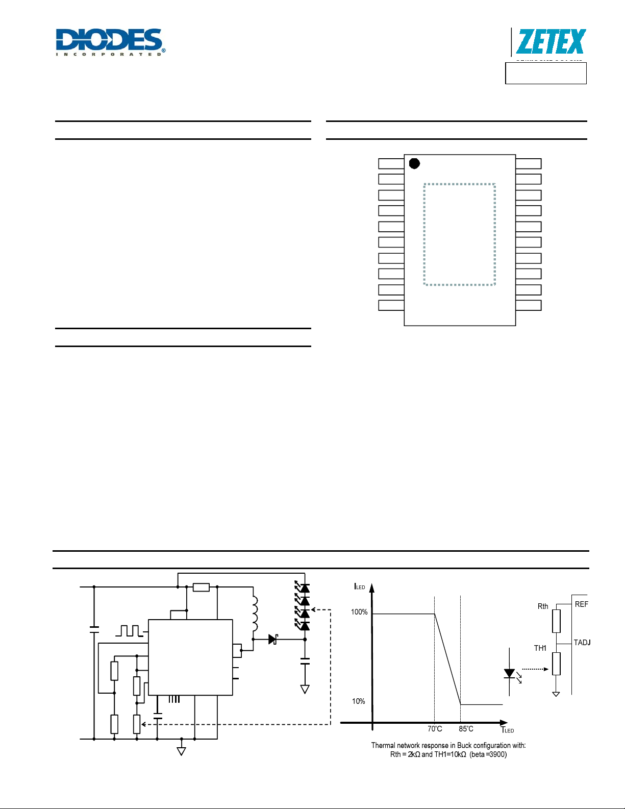
Pin Assignments
ADJ 1
REF 2
TA D J 3
SHP 4
STATUS 5
SGND 6
PGND 7
PGND 8
N/C 9
N/C 10
Thermal
Pad
20 GI
19 PWM
18 FLAG
17 ISM
16 VIN
15 VAUX
14 LX
13 LX
12 N/C
11 N/C
Typical Applications Circuit
V
IN
GND
C1
RGI2
RGI2
R4
TH1
VAUX V IN IS M
PWM
GI
ADJ
REF
TADJ
SHP SGND PGND
C2
100pF
ZXLD1374
NC
R1
STATUS
LX
LX
FLAG
L1
SD1
PSD3200
C
OUT
ZXLD1374
Document number: DS35032 Rev. 3 - 2
1 of 39
www.diodes.com
September 2012
© Diodes Incorporated
A
f
Product Line o
Diodes Incorporated
ZXLD1374
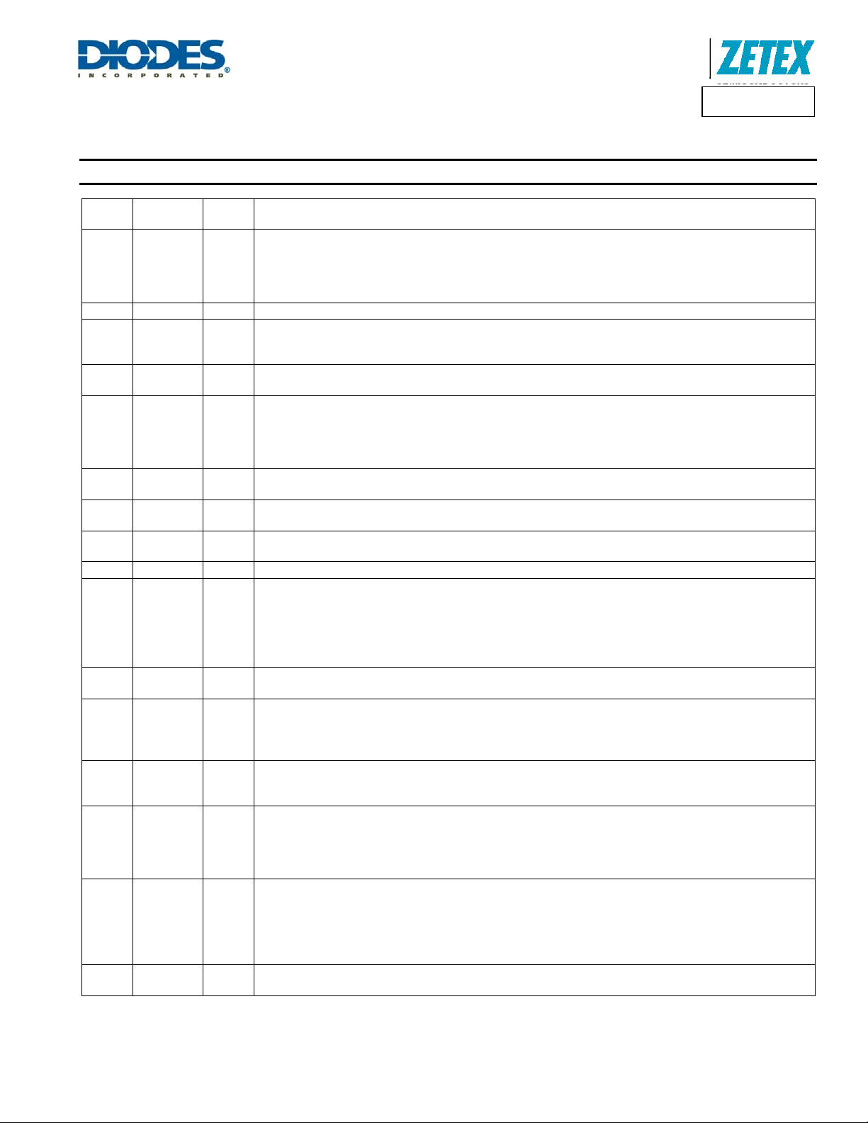
Pin Descriptions
Pin
Name
Pin
ADJ 1 I
REF 2 O Internal 1.25V reference voltage output
T
ADJ
3 I
SHP 4 I/O
STATUS 5 O
SGND 6 P
PGND 7, 8 P
N/C 9, 10, 11, 12 —
LX 13, 14 O Low-Side Power-Switch Output
V
VIN
AUX
15 P
16 P
ISM 17 I
FLAG 18 O
PWM 19 I
GI 20 I
EP PAD P
Note: 4. Type refers to whether or not pin is an Input, Output, Input/Output or Power supply pin.
ZXLD1374
Document number: DS35032 Rev. 3 - 2
Type
(Note 4)
Function
Adjust Input (for DC Output Current Control).
Connect to REF to set 100% output current.
Drive with dc voltage (125mV<V
ADJ pin has an internal clamp that limits the internal
< 2.5V) to adjust output current from 10% to 200% of set value. The
ADJ
node to less than 3V. This prevents the LED and power
switch from delivering too much current should ADJ get overdriven.
Temperature Adjust (Input for LED Thermal Current Control).
Connect thermistor/resistor network to this pin to reduce output current above a preset temperature threshold.
Connect to REF to disable thermal compensation function (See section on thermal control).
Shaping capacitor for feedback control loop.
Connect 100pF ±20% capacitor from this pin to ground to provide loop compensation
Operation Status Output (analog output).
Pin is at 4.5V (nominal) during normal operation.
Pin switches to a lower voltage to indicate specific operation warnings or fault conditions (See section on
STATUS output).
Status pin voltage is low during shutdown mode.
Signal Ground.
Connect to 0V and pins 7 and 8.
Power Ground.
Connect to 0V and pin 6 to maximize copper area.
Not Connected Internally.
To maximize PCB copper for thermal dissipation connect to pins 7 and 8.
Auxiliary Positive Supply to Internal Switch Gate Driver.
Connect to V
, or auxiliary supply from 6V to 15V supply to reduce internal power dissipation (Refer to
IN
application section for more details).
>24V; to reduce power dissipation, V
At V
IN
can be connected to a 12V to 15V auxiliary power supply
AUX
(see Applications section).
Decouple to ground with capacitor close to device (refer to Applications section).
Input Supply to Device (6.3V to 60V).
Decouple to ground with capacitor close to device (refer to Applications section).
Current Monitor Input.
Connect current sense resistor between this pin and V
The nominal voltage, V
, across the resistor is 218mV fixed in Buck mode and initially 225mV in Boost
SENSE
IN.
and Buck-Boost modes, varying with duty cycle.
Flag Open Drain Output.
Pin is high impedance during normal operation.
Pin switches low to indicate a fault, or warning condition.
Digital PWM Output Current Control.
Pin driven either by open Drain or push-pull 3.3V or 5V logic levels.
Drive with frequency higher than 100Hz to gate output ‘on’ and ‘off’ during dimming control.
The device enters standby mode when PWM pin is driven with logic low level for more than 15ms nominal
(Refer to application section for more details).
Gain Setting Input.
Used to set the LED current in Boost and Buck-Boost modes.
In
Buck mode operation the GI pin must be connected to ADJ.
For
Boost and Buck-boost modes, connect to resistive divider from ADJ to SGND. This defines the ratio of
switch current to LED current (see application section). The GI pin has an internal clamp that limits the
internal
node to less than 3V. This provides some failsafe should the GI pin get overdriven.
Exposed Pad.
Connect to 0V plane for electrical and thermal management.
2 of 39
www.diodes.com
September 2012
© Diodes Incorporated
A
f
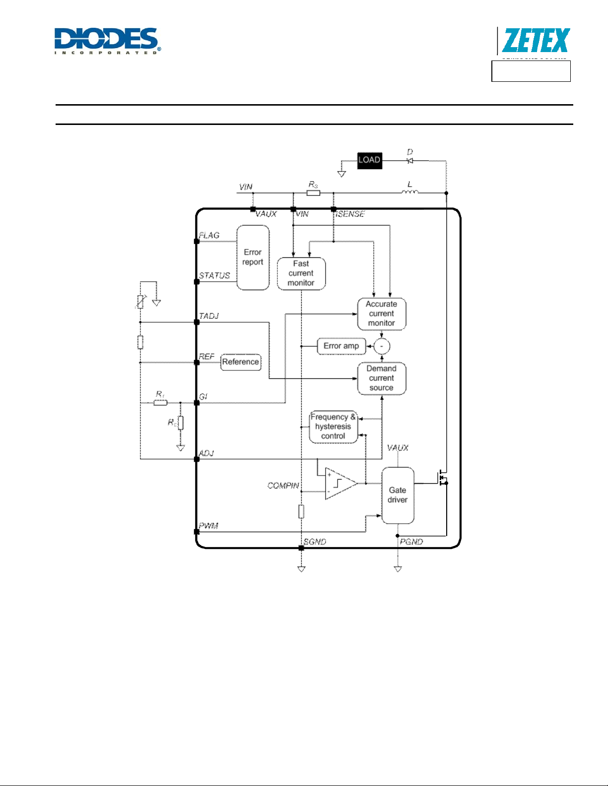
Functional Block Diagram
Product Line o
Diodes Incorporated
ZXLD1374
ZXLD1374
Document number: DS35032 Rev. 3 - 2
3 of 39
www.diodes.com
September 2012
© Diodes Incorporated
A
f
Product Line o
Diodes Incorporated
ZXLD1374
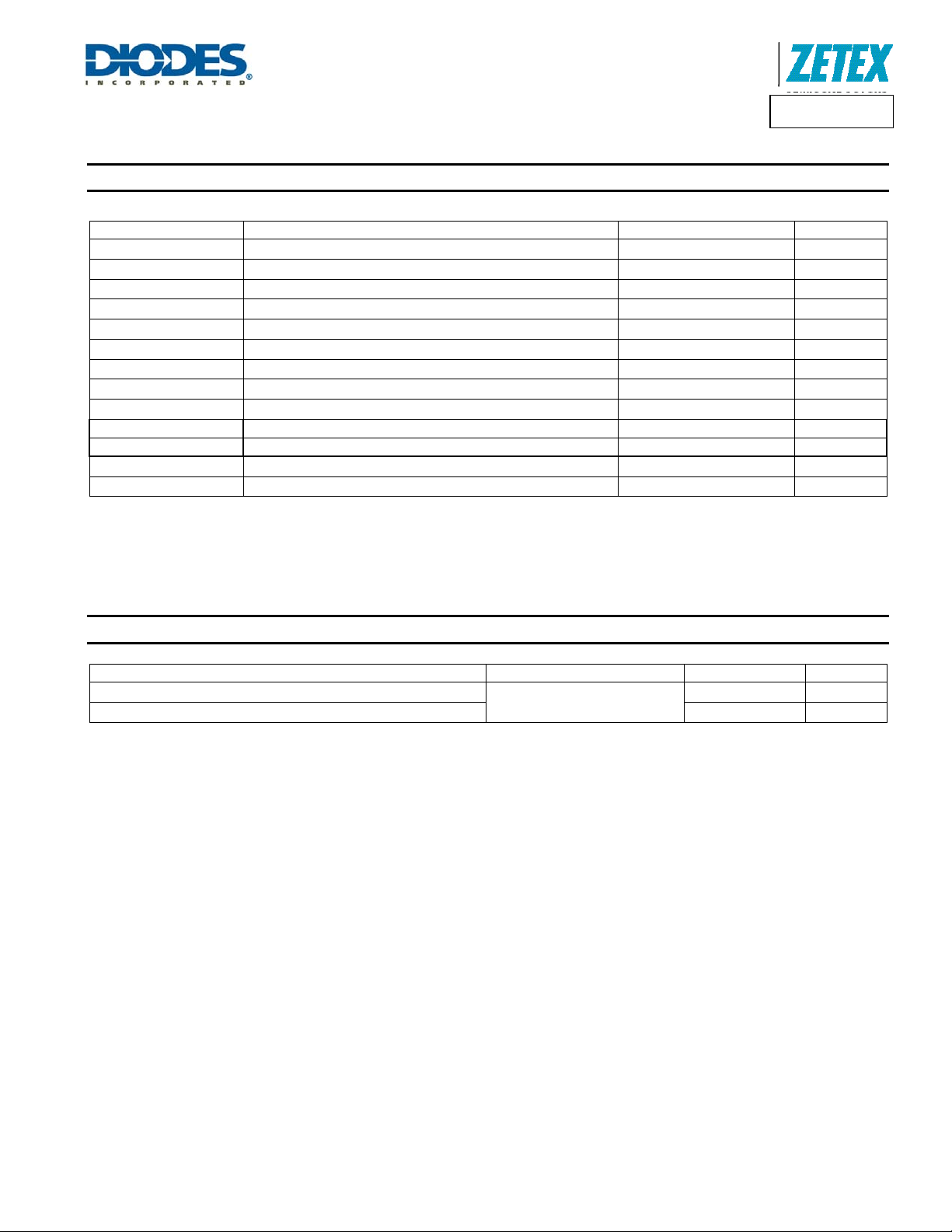
Absolute Maximum Ratings (Voltages to GND unless otherwise specified.)
Symbol Parameter Rating Unit
‡
-0.3 to +65 V
‡
-0.3 to +65 V
‡
-0.3 to +65 V
)
ISM
‡
-0.3 to +65 V
-0.3 to +5 V
V
PWM
, V
VIN
V
AUX
V
ISM
V
Current Monitor Sense Voltage (VIN-V
SENSE
VLX
ILX
I
STATUS
V
FLAG
, V
ADJ
TADJ
Input Supply Voltage Relative to GND
Auxiliary Supply Voltage Relative to GND
Current Monitor Input Relative to GND
Low Side Switch Output Voltage to GND
Low Side Switch Continuous Output Current 1.8 A
Status Pin Output Current ±1 mA
Flag Output Voltage to GND (Note 5) -0.3 to +40 V
Other Input Pins to GND (Note 5) -0.3 to +5.5 V
, VGI
ESD HBM Human Body Model ESD Protection 500 V
ESD CDM Charged Device Model ESD Protection 1000 V
TJ
TST
Note: 5. For correct operation SGND and PGND should always be connected together.
These are stress ratings only. Operation outside the absolute maximum ratings may cause device failure.
Operation at the absolute maximum rating for extended periods may reduce device reliability.
Semiconductor devices are ESD sensitive and may be damaged by exposure to ESD events. Suitable ESD precautions should be taken when handling and
transporting these devices.
Maximum Junction Temperature 150 °C
Storage Temperature -55 to +150 °C
Package Thermal Data
Junction-to-Ambient, JA (Note 6)
Junction-to-Case, JC
Note: 6. Measured on High Effective Thermal Conductivity Test Board" according JESD51.
ZXLD1374
Document number: DS35032 Rev. 3 - 2
Thermal Resistance Package Unit
TSSOP-20EP
4 of 39
www.diodes.com
28 °C/W
4 °C/W
September 2012
© Diodes Incorporated
A
f
Product Line o
Diodes Incorporated
ZXLD1374
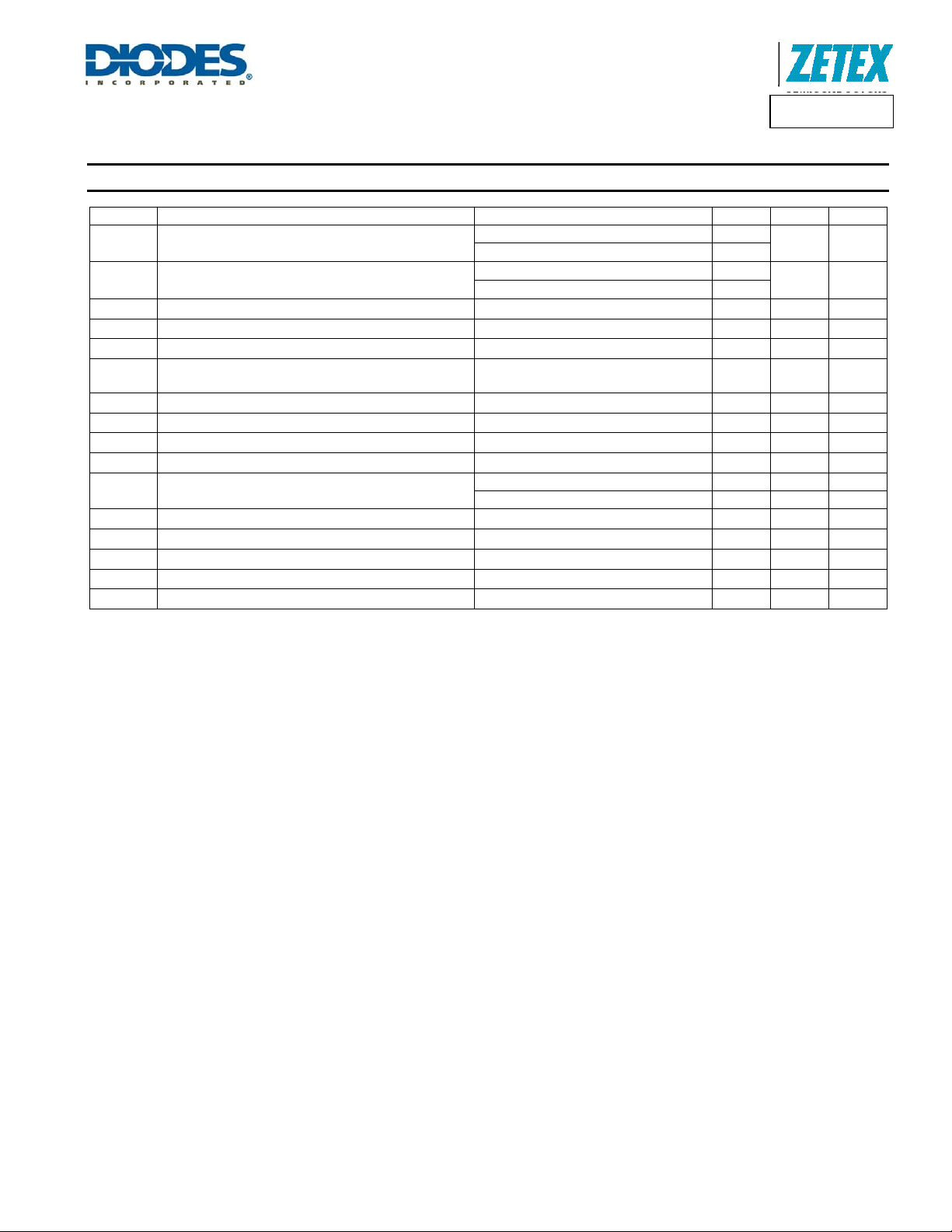
Recommended Operating Conditions (@T
Symbol Parameter Performance/Comment Min Max Unit
Input Supply Voltage Range
VIN
V
V
SENSE
V
I
STATUS
I
V
f
t
PWMH/L
V
V
Notes: 7. Device is guaranteed to have started up by 6.5V and as such the minimum applied supply voltage has to be above 6.5V (plus any noise margin).
The ZXLD1374 will, however, continue to function when the input voltage is reduced from ≥ 8V down to 6.3V.
When operating with input voltages below 8V the output current and device parameters may deviate from their normal values; and is dependent on
power MOSFET switch, load and ambient temperature conditions. To ensure best operation in Boost and Buck-boost modes with input voltages, V
between 6.5 and 12V a suitable boot-strap network on V
V
8. V
be applied to V
9. The device contains circuitry to control the switching frequency to approximately 400kHz. The maximum and minimum operating frequency is not
tested.
ZXLD1374
Document number: DS35032 Rev. 3 - 2
Auxiliary Supply Voltage Range (Note 8)
AUX
Differential Input Voltage
Low Side Switch Output Voltage 60 V
VLX
Low Side Switch Continuous Output Current 1.5 A
ILX
External DC Control Voltage Applied to ADJ Pin to
ADJ
Adjust Output Current
Status Pin Output Current 100 µA
Reference External Load Current REF sourcing current 1 mA
REF
Recommended Switching Frequency Range (Note 9) 300 1000 kHz
fSW
Temperature Adjustment (T
TADJ
Recommended PWM Dimming Frequency Range
PWM
PWM Pulse Width in Dimming Mode PWM input high or low 0.005 10 ms
PWM Pin High Level Input Voltage 2 5.5 V
PWMH
PWM Pin Low Level Input Voltage 0 0.4 V
PWML
Operating Junction Temperature Range -40 +125 °C
TJ
) Input Voltage Range
ADJ
GI Gain Setting Ratio for Boost and Buck-Boost Modes
) below 8V. – A boot-strap network cannot be implemented in buck mode.
AUX
can be driven from a voltage higher than VIN to provide higher efficiency at low VIN voltages, but to avoid false operation; a voltage should not
AUX
in the absence of a voltage at VIN.
AUX
= +25°C, unless otherwise specified.)
A
Normal operation 8
Reduced performance operation (Note 7) 6.3
Normal operation 8
Reduced performance operation (Note 7) 6.3
V
VIN-VISM
, with 0 V
ADJ
2.5
DC brightness control mode
from 10% to 200%
0 450 mV
0.125 2.5 V
0
60 V
60 V
V
REF
V
To maintain 1000:1 resolution 100 500 Hz
To maintain 200:1 resolution 100 1000 Hz
Ratio= V
pin is recommended. Performance in Buck mode will be reduced at input voltages (VIN,
AUX
GI/VADJ
5 of 39
www.diodes.com
0.20 0.50
,
IN
September 2012
© Diodes Incorporated
A
f
Product Line o
Diodes Incorporated
ZXLD1374
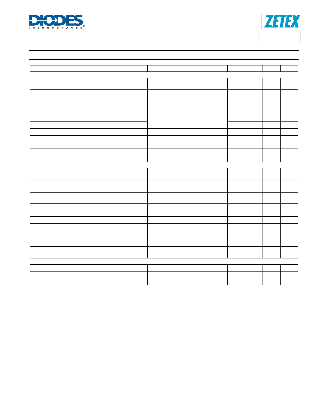
Electrical Characteristics (V
Symbol Parameter Conditions Min Typ Max Units
IN
= V
= 12V, @TA = +25°C, unless otherwise specified.)
AUX
Supply and Reference Parameters
V
V
I
Q-IN
I
Q-AUX
I
SB-IN
I
SB-AUX
V
ΔV
V
REF_LINE
V
REF-TC
Under-Voltage Detection Threshold
UV-
Normal Operation to Switch Disabled
Under-Voltage Detection Threshold
UV+
Switch Disabled to Normal Operation
Quiescent Current into VIN
Quiescent Current into V
Standby Current into VIN.
Standby Current into V
Internal Reference Voltage No load 1.237 1.25 1.263 V
REF
Change in Reference Voltage with Output
REF
Current
Reference Voltage Line Regulation
Reference Temperature Coefficient
AUX
AUX
VIN or V
VIN or V
falling (Note 10)
AUX
rising (Note 10)
AUX
PWM pin floating.
.
Output not switching
PWM pin grounded for more than 15ms
5.2 5.6 6.3
5.5 6 6.5
1.5 3
150 300
90 150
0.7 10
Sourcing 1mA -5
Sinking 25µA 5
VIN = V
, 6.5V < VIN = <60V
AUX
-60 -90
+/-50
V
V
mA
µA
µA
µA
mV
dB
ppm/°C
DC-DC Converter Parameters
V
ADJ
I
ADJ
VGI
IGI
I
PWM
t
PWMoff
T
SDH
T
SDL
External DC Control Voltage Applied to ADJ Pin
to Adjust Output Current (Note 11)
ADJ Input Current (Note 11)
GI Voltage Threshold for Boost and Buck-Boost
Modes Selection (Note 11)
GI Input Current (Note 11)
PWM Input Current
PWM Pulse Width
(to enter shutdown state)
Thermal Shutdown Upper Threshold
(LX output inhibited)
Thermal Shutdown Lower Threshold
(LX output re-enabled)
DC brightness control mode
10% to 200%
2.5V
V
ADJ
= 5.0V
V
ADJ
V
= 1.25V
ADJ
2.5V
V
GI
= 5.0V
V
GI
V
= 5.5V
PWM
0.125 1.25 2.5 V
100
5
nA
µA
0.8 V
100
5
nA
µA
36 100 µA
PWM input low 10 15 25 ms
Temperature rising 150 °C
Temperature falling 125 °C
High-Side Current Monitor (Pin ISM)
I
ISM
V
SENSE_acc
V
SENSE-OC
Notes: 10. UVLO levels are such that all ZXLD1374 will function above 6.5V for rising supply voltages and function down to 6.3V for falling supply voltages.
overdriven.
Input Current
Accuracy of Nominal V
Over-Current Sense Threshold Voltage 300 350 375 mV
11. The ADJ and GI pins have an internal clamp that limits the internal node to less than 3V. This limits the switch current should those pins get
Threshold Voltage
SENSE
Measured into ISM pin and V
V
= 1.25V
ADJ
ISM
= VIN
11 20 µA
±0.25 ±2 %
ZXLD1374
Document number: DS35032 Rev. 3 - 2
6 of 39
www.diodes.com
September 2012
© Diodes Incorporated
A
f
Product Line o
Diodes Incorporated
ZXLD1374
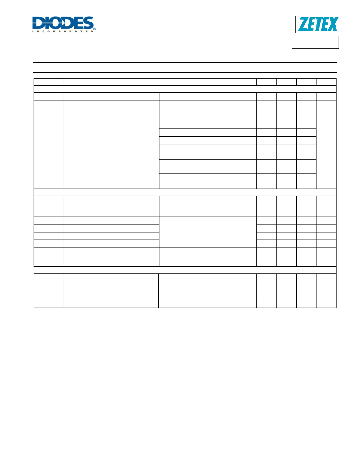
Electrical Characteristics (cont.) (V
Symbol Parameter Conditions Min Typ Max Units
Output Parameters
V
FLAGL
I
FLAGOFF
V
STATUS
R
STATUS
Low Side Switch Output (LX pins tied together)
I
LX-LG
R
DS(ON)
t
PDHL
t
PDLH
t
LXR
t
LXF
t
STALL
LED Thermal control circuit (TADJ) parameters
V
TADJH
V
TADJL
I
TADJ
Notes: 12. Flag is asserted if V
13. In the event of more than one fault/warning condition occurring, the higher priority condition will take precedence. E.g. ‘Excessive coil current’
and ‘Out of regulation’ occurring together will produce an output of 0.9V on the STATUS pin. The voltage levels on the STATUS output assume
the Internal regulator to be in regulation and V
this is due to the feedback loop increasing the sense voltage.
14. With the device still in switching mode the LX pin has an over-voltage detection circuit connected to it with a resistance of approximately 1MΩ.
15. If t
switched to its nominal operating voltage, before operation is allowed to resume. Restart cycles will be repeated automatically until the operating
conditions are such that normal operation can be sustained. If t
ZXLD1374
Document number: DS35032 Rev. 3 - 2
FLAG Pin Low Level Output Voltage Output sinking 1mA 0.5 V
FLAG Pin Open-Drain Leakage Current
STATUS Flag No-Load Output Voltage
(Note 13)
Output Impedance of STATUS Output Normal operation 10 k
Low Side Switch Leakage Current
LX Pin MOSFET on Resistance
Propagation Delay High-Low
Propagation Delay Low-High 131 ns
LX Output Rise Time 208 ns
LX Output Fall Time 12 ns
Time to assert ‘STALL’ flag and
warning on STATUS output
(Note 15)
Upper Threshold Voltage
Lower Threshold Voltage
TADJ Pin Input Current
<2.5V or V
exceeds t
ON
SHP
, LX turns off and then an initiate a restart cycle occurs. During this phase, ADJ is grounded internally and the SHP pin is
STALL
SHP
>3.5V
IN
= V
= 12V, @TA = +25°C, unless otherwise specified.)
AUX
V
FLAG
= 40V
1 µA
Normal operation 4.2 4.5 4.8
Out of regulation (V
(Note 12)
VIN under-voltage (V
Switch stalled (tON or t
LX over-voltage state (VLX > 60V)
Over-temperature (TJ > 125°C)
Excess sense resistor current
SENSE
> 0.375V)
(V
Excessive switch current (ISW>1.5A)
Output stage off, V
(Note 14)
ILX = 1.5A (tON < 100µs)
out of range)
SHP
< 5.6V)
IN
> 100µs)
OFF
= 60V
LX
3.3 3.6 3.9
3.3 3.6 3.9
3.3 3.6 3.9
2.4 2.7 3.0
1.5 1.8 2.1
0.6 0.9 1.2
0.6 0.9 1.2
60 µA
0.5 0.8
86 ns
V
= 225mV ± 30%, CL = 680pF,
SENSE
R
= 120Ω
L
LX low or high 100 170 µs
Onset of output current reduction (V
falling)
Output current reduced to <10% of set value
(V
falling)
TADJ
V
= 1.25V
TADJ
<=V
ADJ
. A reduction of the voltage on the STATUS pin will occur when the voltage on VIN is near –
REF
exceeds t
OFF
, the switch will remain off until normal operation is possible.
STALL
TADJ
560 625 690 mV
380 440 500 mV
1 µA
7 of 39
www.diodes.com
V
Ω
September 2012
© Diodes Incorporated
A
f
U
Y CUR
R
C
R
Q
C
CUR
RENT
Product Line o
Diodes Incorporated
ZXLD1374
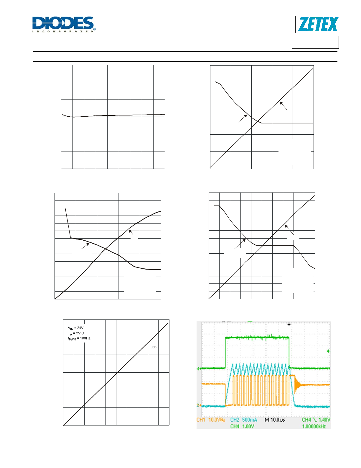
Typical Characteristics
3
2.5
1500
1250
900
750
SWITCHING FREQUENCY (kHz)
2
ENTt (mA)
1.5
1
PPL
S
0.5
0
6 1218 24 303642 485460
SUPPLY VOLTAGE (V)
Figure 1 Supply Current vs. Supply Voltage
700
1400
650
600
1200
550
500
1000
450
400
I
LED
800
350
300
Switc hing
Frequency
600
250
LED CURRENT (mA)
200
T = 25°C
150
100
50
0
0 0.5 1 1.5 2 2.5
ADJ VOLTAGE
A
V = V = 24V
AUX IN
8LEDs
µ
L = 33 H
GI = 0.23
R = 300m
S
400
200
Ω
0
Figure 3 Buck-Boost LED Current, Switching Frequency vs. V
1500
ADJ
SWITCHING FREQUENCY (kHz)
1000
I
LED
750
Switching
500
LED CURRENT (mA)
250
0
Frequency
T = 25°C
A
V = V = 12V
AUX IN
2LEDs
µ
L = 33 H
Ω
R = 300m
S
0
0.5
ADJ VOLTAGE (V)
1
1.5
2
Figure 2 Buck LED Current, Switching Frequency vs. V
700
650
600
550
500
450
(mA)
400
I
LED
350
300
Switching
Frequency
250
LED
200
150
100
50
0
0 0.25 0.5 0.75 1 1.25 1.5 1.75 2 2.25 2.5
ADJ VOLTAGE
T = 25°C
A
V = V = 12V
AUX IN
12 LEDs
µ
L = 33 H
Ω
R = 300m
S
Figure 4 Boost LED Current, Switching Frequency vs. V
2.5
600
450
300
150
0
ADJ
700
600
500
400
300
200
100
ADJ
SWIT
HING F
E
UEN
Y(kHz)
0
1250
1000
750
500
LED CURRENT (mA)
250
0
0 102030405060708090100
PWM DUTY CYCLE (%)
Figure 5 I vs. PWM Duty Cycle
LED
Figure 6 I
vs. Time - PWM Pin Transient Response
LED
ZXLD1374
Document number: DS35032 Rev. 3 - 2
8 of 39
www.diodes.com
September 2012
© Diodes Incorporated
A
f
C
U
R
REN
T
N
G FACTO
R
REFERENC
OLTAG
P
O
R
TCH ON-R
TANC
UTY
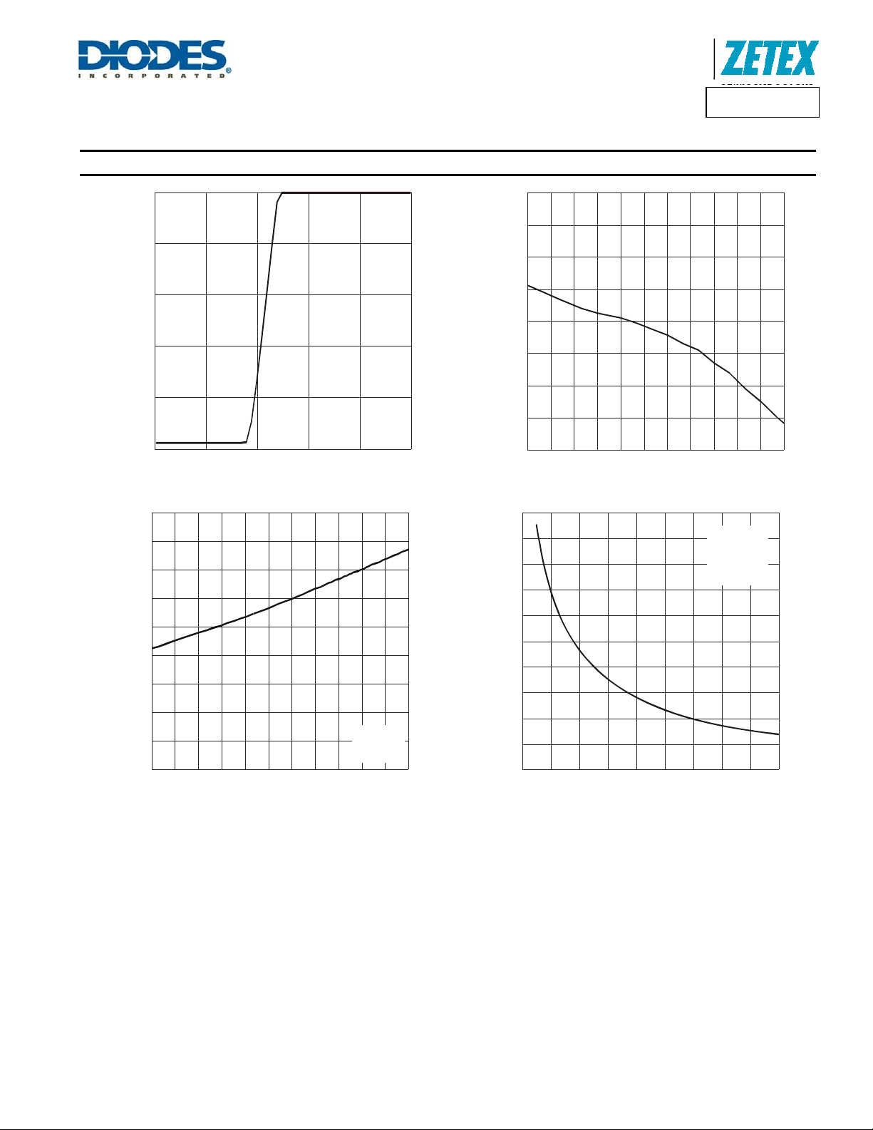
Typical Characteristics (cont.)
100%
80%
60%
DIMMI
40%
Product Line o
Diodes Incorporated
ZXLD1374
1.252
1.2515
1.251
E (V)
1.2505
1.25
E V
1.2495
20%
1.249
LED
0%
0 250 500 750 1000 1250
T PIN VOLTAGE (mV)
ADJ
Figure 7 LED Current vs. T Voltage
ADJ
0.9
0.8
Ω
E ( )
0.7
0.6
ESIS
0.5
1.2485
1.248
-40 -25 -10 5 20 35 50 65 80 95 110 125
JUNCTION TEMPERATURE (°C)
Figure 8 V vs. Temperature
REF
100%
T = 25C
90%
80%
A
L = 33µH
R = 150m
S
Buck Mode
2 LEDS
70%
60%
°
Ω
50%
0.4
D
40%
0.3
SWI
0.2
WE
0.1
0
-40 -25 -10 5
V = 12V
I = 1.3A
LX
20 35 50 65 80 95 110 125
JUNCTION TEMPERATURE (°C)
Figure 9 R vs. Temperature
DS(ON)
IN
30%
20%
10%
0%
6 121824303642485460
INPUT VOLTAGE (V)
Figure 10 Duty Cycle vs. Input Voltage
ZXLD1374
Document number: DS35032 Rev. 3 - 2
9 of 39
www.diodes.com
September 2012
© Diodes Incorporated
A
f
ED CURRENT
TCH
REQ
UENC
Y
H
C
C
Y
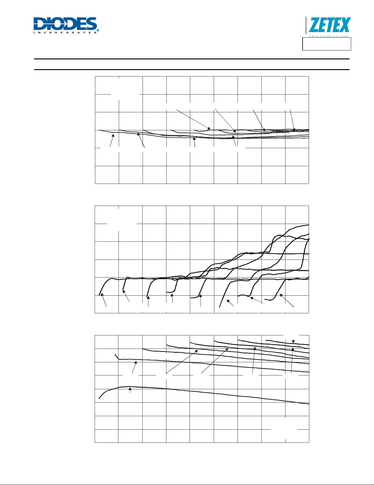
Typical Characteristics – Buck Mode – R
1.65
T = 25°C
A
V = V
AUX IN
1.60
1.55
(A)
L = 33µH
R = 146m
S
Ω
1.50
1.45
L
1 LED
3 LEDs 5 LEDs
1.40
= 146m, L = 35µH, I
S
9 LEDs
= 1.5A
LED
11 L ED s
Product Line o
Diodes Incorporated
13 LEDs
7 LEDs
ZXLD1374
15 LEDs
1.35
61218243036424854
INPUT VOLTAGE (V)
Figure 11 Load Current vs. Input Voltage and Number of LED
1200
T = 25°C
A
V = V
AUX IN
1000
z)
L = 33µ H
R = 146m
S
Ω
(k
800
600
ING F
400
SWI
200
1 LED
0
6 12182430 3642485460
3 LEDs
5 LEDs
7 LEDs
INPUT VOLTAGE (V)
11 L E Ds9 LEDs
13 LEDs
15 LEDs
Figure 12 Frequency vs. Input Voltage and Number of LED
100%
15 LEDs
95%
5 LEDs
90%
60
IEN
EFFI
85%
80%
75%
3 LEDs
1 LED
11 L EDs9 LEDs7 LEDs
13 LEDs
70%
T = 25°C
A
V = V
65%
60%
6
12 18 24 30 36 42 48 54 60
AUX IN
L = 33µ H
R = 146m
S
Ω
Input Voltage (V)
Figure 13 Efficiency vs. Input Voltage and Number of LED
ZXLD1374
Document number: DS35032 Rev. 3 - 2
10 of 39
www.diodes.com
September 2012
© Diodes Incorporated
A
f
F
F
CIENCY
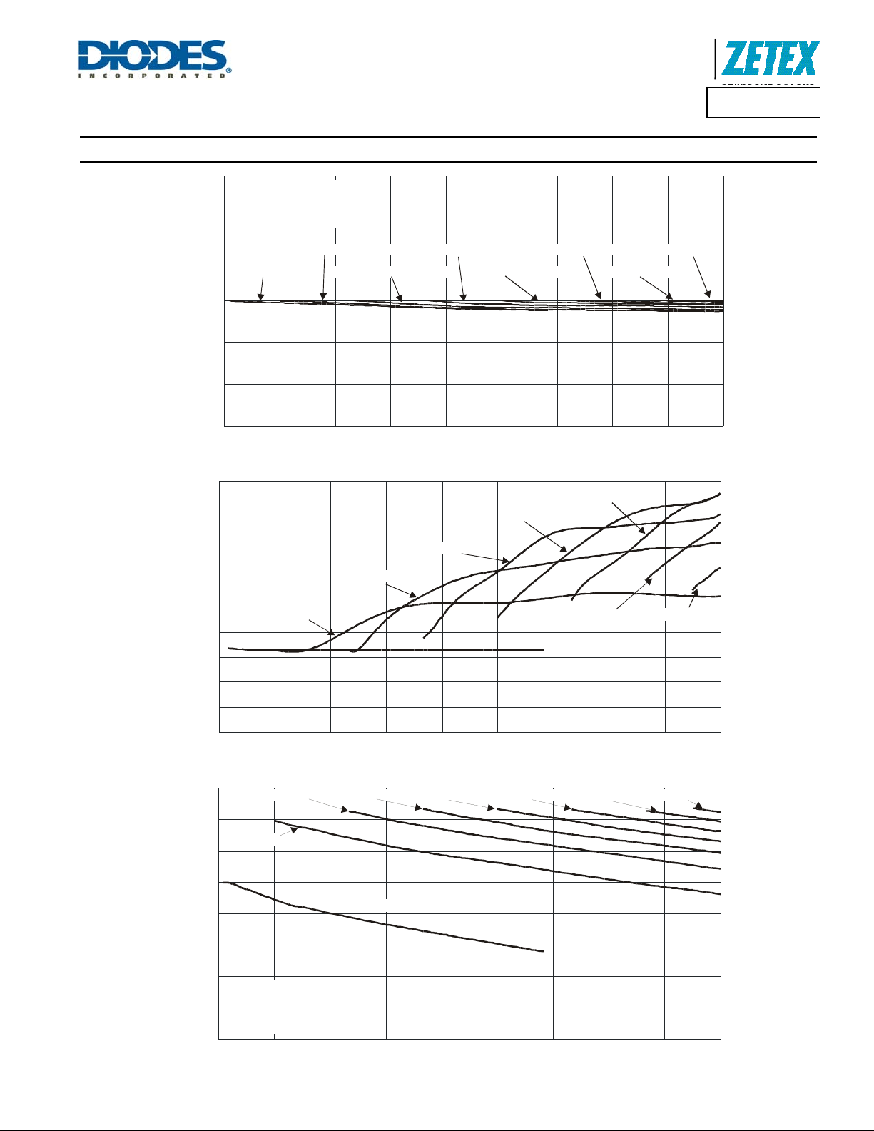
Typical Characteristics – Buck Mode – R
0.825
0.800
T = 25°C
A
V = V
AUX IN
L = 33µ H
R = 291m
S
Ω
= 291m, L = 35µH, I
S
= 750mA
LED
Product Line o
Diodes Incorporated
ZXLD1374
0.775
1 LED
3 LEDs
5 LEDs
7 LEDs 11 LEDs
9 LEDs
13 LEDs
15 LEDs
0.750
LED CURRENT (A)
0.725
0.700
0.675
6 12182430 3642 4854 60
INPUT VOLTAGE (V)
1000
900
800
700
600
500
T = 25°C
A
V = V
AUX IN
L = 33µ H
R = 291m
S
Figure 14 I vs. Input Voltage and Number of LED
Ω
3 LEDs
5 LEDs
LED
7 LEDs
9 LEDs
11 L EDs
13 LEDs
15 LEDs
400
FREQUENCY (kHz)
300
1 LED
200
100
100%
0
6
12 18 24 30 36 42 48
Figure 15 Frequency ZXLD1374 - Buck Mode = L = 47 H
5 LEDs
7 LEDs
INPUT VOLTAGE (V)
9 LEDs
11 L ED s
μ
13 LEDs
54
15 LEDs
60
95%
90%
3 LEDs
85%
1 LED
I
E
80%
75%
70%
T = 25°C
A
V = V
65%
60%
6
AUX IN
L = 33µ H
R = 291m
S
12
Ω
18
24
30 36
42
48 54 60
INPUT VOLTAGE (V)
Figure 16 Efficiency vs. Input Voltage and Number of LED
ZXLD1374
Document number: DS35032 Rev. 3 - 2
11 of 39
www.diodes.com
September 2012
© Diodes Incorporated
A
f
ED CURRENT
REQ
UENC
Y
H
C
N
C
Y
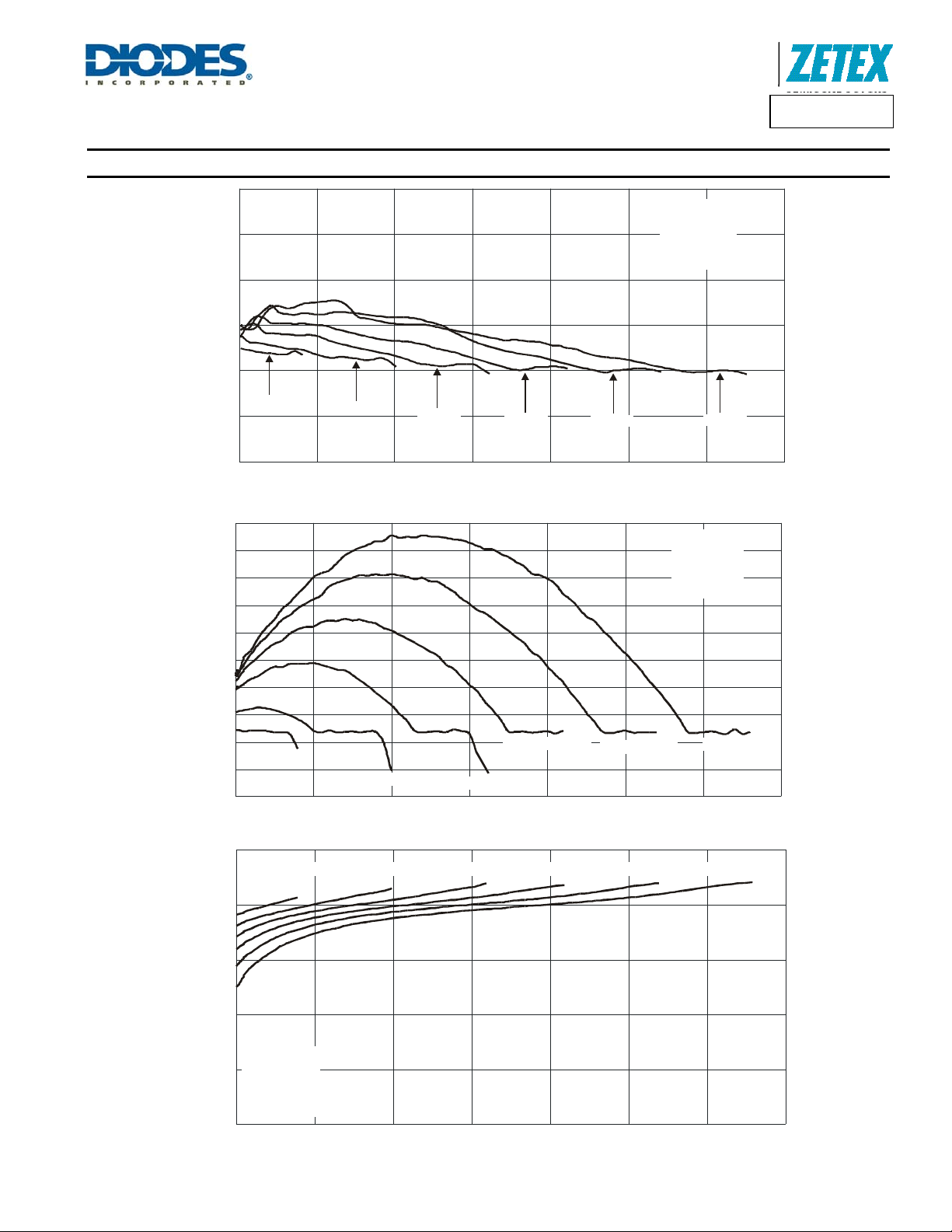
Typical Characteristics – Boost Mode – R
0.358
0.347
0.336
(A)
0.325
0.314
L
= 150m, L = 33µH, I
S
= 325mA, GI
LED
Product Line o
Diodes Incorporated
= 0.21
RATIO
°
T = 25C
A
L = 33µ H
Ω
R = 150m
S
R = 33k
Ω
GI1
R = 120k
GI2
Ω
ZXLD1374
0.303
6 LEDs
0.292
12 17 22 27 32
8 LEDs
10 LEDs
INPUT VOLTAGE (V)
Figure 17 I vs. Input and Number of LED
LED
700
650
600
z)
550
(k
500
450
400
F
350
300
250
200
6 LEDs
8 LEDs
12 17 22
10 LEDs
27 32 37 42 47
INPUT VOLTAGE (V)
Figure 18 Frequency vs. Input Voltage and Number LED
100%
12 LEDs
12 LEDs
14 LEDs
16 LEDs
37 42 47
T = 25C
°
A
L = 33µ H
R = 150m
Ω
S
R = 33k
Ω
GI1
R = 120k
GI2
14 LEDs
Ω
16 LEDs
16 LEDs14 LEDs12 LEDs10 LEDs8 LEDs6 LEDs
95%
90%
IE
85%
EFFI
T = 25C
°
A
L = 33µH
80%
75%
12 17 22 27 32 37 42 47
R = 150m
S
R = 33k
GI1
R = 120k
GI2
Ω
Ω
Ω
INPUT VOLTAGE (V)
Figure 19 Efficiency vs. Input Voltage and Number of LED
ZXLD1374
Document number: DS35032 Rev. 3 - 2
12 of 39
www.diodes.com
September 2012
© Diodes Incorporated
 Loading...