

Page 1
A
Product Line o
f
Diodes Incorporated
ZXLD1362
Description
The ZXLD1362 is a continuous mode inductive step-down converter
with integrated switch and high side current sense.
It operates from an input supply from 6V to 60V driving single or
multiple series connected LEDs efficiently externally adjustable
output current up to 1A.
The ZXLD1362 has been qualified to AEC-Q100 Grade 1 enabling
operation in ambient temperatures from -40°C to +125°C.
The output current can be adjusted by applying a DC voltage or a
PWM waveform. 100.1 adjustment of output current is possible
using PWM control.
Applying 0.2V or lower to the ADJ pin turns the output off and
switches the device into a low current standby state.
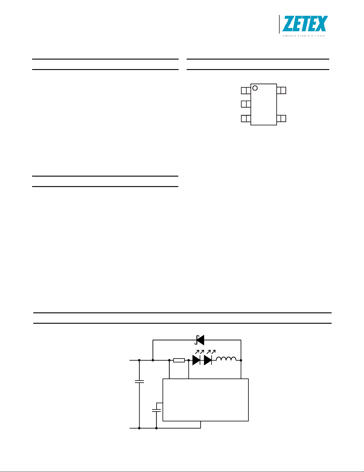
Pin Assignments
Features
• Simple low parts count
• Single pin on/off and brightness control using DC voltage or
PWM
• High efficiency (up to 95%)
• Wide input voltage range: 6V to 60V
• Up to 1MHz switching frequency
• Qualified to AEC-Q100 Grade 1
• Typical 2% output current accuracy
• Thermally enhanced TSOT25:
• Available in Green molding
Totally Lead-Free & Fully RoHS Compliant (Notes 1 & 2)
Halogen and Antimony Free. “Green” Device (Note 3)
Notes: 1. No purposely added lead. Fully EU Directive 2002/95/EC (RoHS) & 2011/65/EU (RoHS 2) compliant.
2. See http://www.diodes.com for more information about Diodes Incorporated’s definitions of Halogen- and Antimony-free, "Green" and Lead-free.
3. Halogen- and Antimony-free "Green” products are defined as those which contain <900ppm bromine, <900ppm chlorine (<1500ppm total Br + Cl)
and <1000ppm antimony compounds.
82°C/W
JA
60V 1A LED DRIVER WITH AEC-Q100
(Top View)
LX
GND
ADJ
TSOT25
V
IN
I
SENSE
Typical Application Circuit
R
V
IN
ADJ
S
0.1Ω
SET
ZXLD1362
GND
V
IN
24V
C1
4.7µF
C2
100nF
GND
ZXLD1362
Document number: DS33472 Rev. 5 - 2
1 of 24
www.diodes.com
L1
68µH
LX
May 2012
© Diodes Incorporated
Page 2
A
f
Pin Description
Name Pin No. Function
LX 1 Drain of NDMOS switch
GND 2 Ground (0V)
Multi-function On/Off and brightness control pin:
• Leave floating for normal operation.(V
ADJ 3
• Drive to voltage below 0.2V to turn off output current
• Drive with DC voltage (0.3V < V
o I
OUTnom
= 0.1/RS)
ADJ
= V
ADJ
REF
< 2.5V) to adjust output current from 25% to 200% of I
• Connect a capacitor from this pin to ground to increase soft-start time.
• Soft-start time increases approximately 200µs/nF.
I
SENSE
VIN
4
Connect resistor R
(Note: R
SMIN
5 Input voltage (6V to 60V). Decouple to ground with 4.7µF of higher X7R ceramic capacitor close to device.
from this pin to VIN to define nominal average output current I
S
= 0.1 with ADJ pin open circuit)
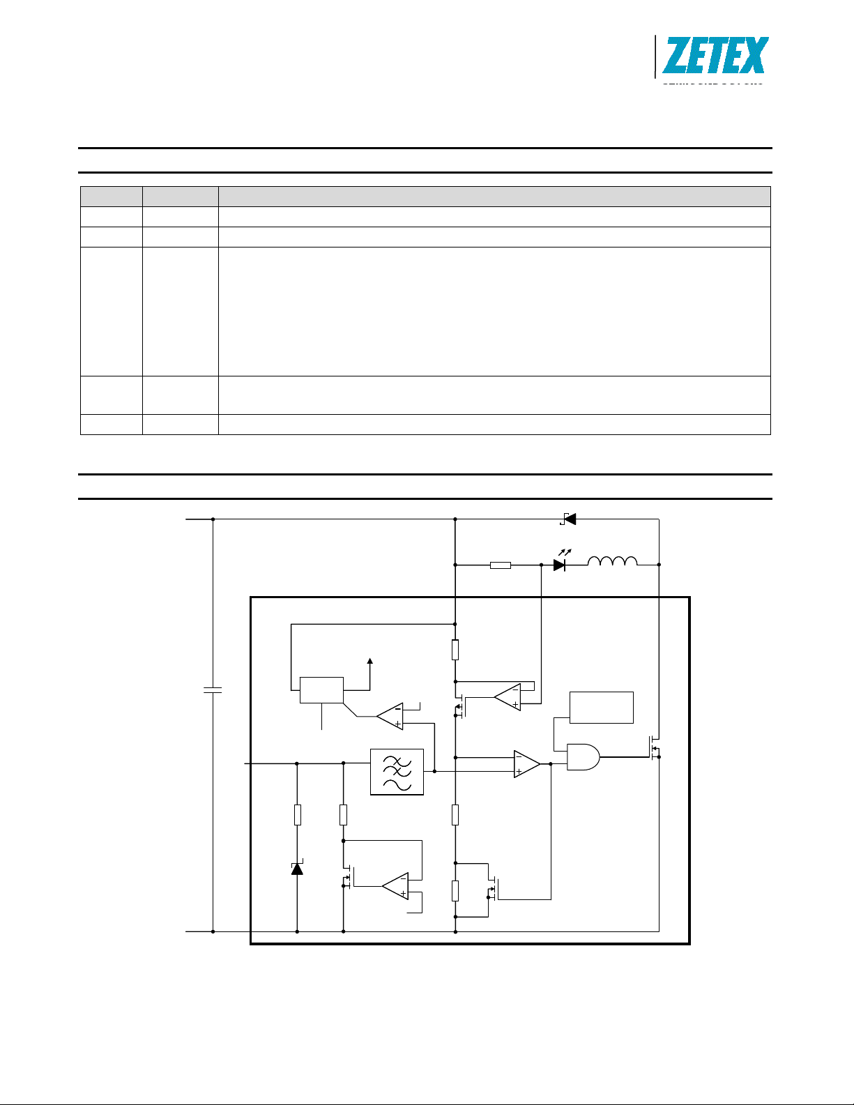
Block Diagram
V
IN
Product Line o
Diodes Incorporated
ZXLD1362
= 1.25V giving nominal average output current
OUTnom
= 0.1/RS
OUTnom
D1
R
S
L1
``
54 1
GND
C1
4.7µF
ADJ
GND
V
IN
5V
Voltage
regulator
GND
3
R4
50k
D1
1.25V
2
R5
20k
1.35V
R1
0.2V
R2
R3
SENSE
Low voltage
detector
LXI
MN
Figure 1. Block Diagram
ZXLD1362
Document number: DS33472 Rev. 5 - 2
2 of 24
www.diodes.com
May 2012
© Diodes Incorporated
Page 3
A
Product Line o
f
Diodes Incorporated
ZXLD1362
Absolute Maximum Ratings (Note 4)
Symbol Parameter Rating Unit
VIN
V
SENSE
VLX
V
ADJ
ILX
P
TOT
TST
TJ
MAX
Note: 4 All voltages unless otherwise stated are measured with respect to GND.
5. V
Caution: Stresses greater than the 'Absolute Maximum Ratings' specified above, may cause permanent damage to the device. These are stress ratings
only; functional operation of the device at conditions between maximum recommended operating conditions and absolute maximum ratings is not
implied. Device reliability may be affected by exposure to absolute maximum rating conditions for extended periods of time.
Input Voltage -0.3 to +65 V
I
Voltage (Note 5)
SENSE
+0.3 to -5 V
LX Output Voltage -0.3 to +65 V
Adjust Pin Input Voltage -0.3 to +6 V
Switch Output Current 1.25 A
Power Dissipation
(Refer to Package thermal de-rating curve on page 16)
1 W
Storage Temperature -55 to +150 °C
Junction Temperature 150 °C
is measured with respect to VIN.
SENSE
ESD Susceptibility
Rating Unit
Human Body Model 500 V
Machine Model 75 V
Caution: Semiconductor devices are ESD sensitive and may be damaged by exposure to ESD events. Suitable ESD precautions should be taken when
handling and transporting these devices.
The human body model is a 100pF capacitor discharge through a 1.5k resistor pin. The machine model is a 200pF capacitor discharged directly
into each pin.
Thermal Resistance
Symbol Parameter Rating Unit
θ
JA
JB
Junction to Ambient 82 °C/W
Junction to Board 33 °C/W
Recommended Operating Conditions
Symbol Parameter Min Max Units
VIN
ILX
V
ADJ
V
ADJoff
t
ONMIN
f
LXmax
DLX
TA
Notes: 6. VIN > 16V to fully enhance output transistor. Otherwise out current must be derated - see graphs. Operation at low supply may cause excessive
heating due to increased on-resistance. Tested at 7V guaranteed for 6V by design.
7. 100% brightness corresponds to V
proportionally.
8. ZXLD1362 will operate at higher frequencies but accuracy will be affected due to propagation delays.
ZXLD1362
Document number: DS33472 Rev. 5 - 2
Input Voltage Range (Note 6) 6 60 V
Maximum recommended continuous/RMS switch current 1 A
External control voltage range on ADJ pin for DC brightness control (Note 7) 0.3 2.5 V
DC voltage on ADJ pin to ensure devices is off 0.25 V
Minimum switch on-time 800 ns
Recommended maximum operating frequency (Note 8) 625 kHz
Duty cycle range 0.01 0.99
Ambient operating temperature range -40 +125 °C
ADJ
= V
ADJ(nom)
= V
. Driving the ADJ pin above V
REF
will increase the V
REF
threshold and output current
SENSE
3 of 24
www.diodes.com
© Diodes Incorporated
May 2012
Page 4
A
Product Line o
f
Diodes Incorporated
ZXLD1362
Electrical Characteristics (Test conditions: V
Symbol Parameter Condition Min Typ Max Unit
VSU
VSD
I
INQoff
I
INQon
V
SENSE
V
SENSEHYS
I
SENSE
V
REF
ΔV
REF
V
ADJ
V
ADJoff
V
ADJon
R
ADJ
I
LXmean
RLX
I
LX(leak)
D
PWM(LF)
DC
tSS
fLX
t
ONmin
t
OFFmin
Notes: 9. Static current of device is approximately 700µA, see Graph, Page 16.
10. Ratio of maximum brightness to minimum brightness before shutdown V
ZXLD1362
Document number: DS33472 Rev. 5 - 2
Internal regulator start-up threshold 4.85 V
Internal regulator shutdown threshold 4.75 V
Quiescent supply current with output off ADJ pin grounded 65 90 µA
Quiescent supply current with output switching
(Note 9)
Mean current sense threshold voltage
(Defines LED current setting accuracy)
Sense threshold hysteresis ±10 %
I
/ΔT Temperature coefficient of V
Resistance between ADJ pin and V
pin input current V
SENSE
Internal reference voltage
REF
External control voltage range on ADJ pin for DC
brightness control (Note 7)
DC voltage on ADJ pin to switch device from active
(on) state to quiescent (off) state
DC voltage on ADJ pin to switch device from
quiescent (off) state to active (on) state
REF
Continuous LX switch current 1 A
LX switch ‘On’ resistance
LX switch leakage current 5 µA
Duty cycle range of PWM signal applied to ADJ pin
during low frequency PWM dimming mode
Brightness control range 1000:1
DC Brightness control range Note 10 5:1
ADJ
Soft start time
Operating frequency
(See graphs for more details)
Minimum switch ‘ON’ time LX switch ‘ON’ 130 ns
Minimum switch ‘OFF’ time LX switch ‘OFF’ 70 ns
= 24V, TA = +25°C, unless otherwise specified.)
IN
ADJ pin floating, L = 68µH,
3 LEDs, f = 260kHz
Measured on I
respect to V
= V
SENSE
IN
SENSE
IN VADJ
-0.1
pin with
= 1.25V
Measured on ADJ pin with
pin floating
1.8 mA
95 100 105 mV
4 10 µA
1.25 V
50 ppm/°C
0.3 2.5 V
V
falling
ADJ
rising
V
ADJ
< V
0 < V
V
ADJ
ADJ
> V
REF
+100mV
REF
@ ILX = 1A
PWM frequency <300Hz
PWM amplitude = V
REF
0.15 0.2 0.27 V
0.2 0.25 0.3 V
30
10.4
50
14.2
65
18
k
0.5 1.0
0.001 1
Measured on ADJ pin
Time taken for output current
to reach 90% of final value
after voltage on ADJ pin has
risen above 0.3V. Requires
2 ms
external capacitor 22nF. See
graphs for more details
ADJ pin floating
L = 68µH (0.1V)
I
= 1A @ V
OUT
LED
= 3.6V
300 kHz
Driving 3 LEDs
= 1.25/0.3. V
REF
4 of 24
www.diodes.com
externally driven to 2.5V, ratio 10:1.
REF
May 2012
© Diodes Incorporated
Page 5
A
f
Diodes Incorporated
Device Description
The device, in conjunction with the coil (L1) and current sense resistor (R
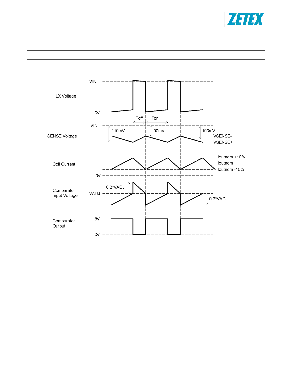
Device operation (refer to Figure 1 - Block diagram and Figure 2 Operating waveforms)
), forms a self-oscillating continuous-mode buck converter.
S
Product Line o
ZXLD1362
Figure 2. Theoretical Operating Waveforms
Operation can be best understood by assuming that the ADJ
pin of the device is unconnected and the voltage on this pin
(V
) appears directly at the (+) input of the comparator.
ADJ
When input voltage V
is zero and there is no output from the current sense
and R
S
is first applied, the initial current in L1
IN
circuit. Under this condition, the (-) input to the comparator is at
ground and its output is high. This turns MN on and switches
the LX pin low, causing current to flow from V
, L1 and the LED(s). The current rises at a rate determined
R
S
and L1 to produce a voltage ramp (V
by V
IN
The supply referred voltage V
is forced across internal
SENSE
to ground, via
IN
SENSE
) across RS.
resistor R1 by the current sense circuit and produces a
proportional current in internal resistors R2 and R3. This
comparator. When this reaches the threshold voltage (V
the comparator output switches low and MN turns off. The
comparator output also drives another NMOS switch, which
bypasses internal resistor R3 to provide a controlled amount of
hysteresis. The hysteresis is set by R3 to be nominally 10% of
.
V
ADJ
When MN is off, the current in L1 continues to flow via D1 and
the LED(s) back to V
. The current decays at a rate
IN
determined by the LED(s) and diode forward voltages to
produce a falling voltage at the input of the comparator. When
this voltage returns to V
, the comparator output switches
ADJ
high again. This cycle of events repeats, with the comparator
input ramping between limits of V
ADJ
± 10%.
ADJ
),
produces a ground referred rising voltage at the (-) input of the
ZXLD1362
Document number: DS33472 Rev. 5 - 2
5 of 24
www.diodes.com
May 2012
© Diodes Incorporated
Page 6
A
f
Device Description
Switching Thresholds
With V
average V
the I
I
OUTnom
I
OUTnom
Nominal ripple current is ±10mV/R
Adjusting output current
The device contains a low pass filter between the ADJ pin and
the threshold comparator and an internal current limiting
resistor (50k nom) between ADJ and the internal reference
voltage. This allows the ADJ pin to be overdriven with either
Actual Operating Waveforms
= V
ADJ
pin with respect to VIN). The average output current
SENSE
is then defined by this voltage and RS according to:
= 100mV/RS
V
IN
, the ratios of R1, R2 and R3 define an
REF
switching threshold of 100mV (measured on
SENSE
S
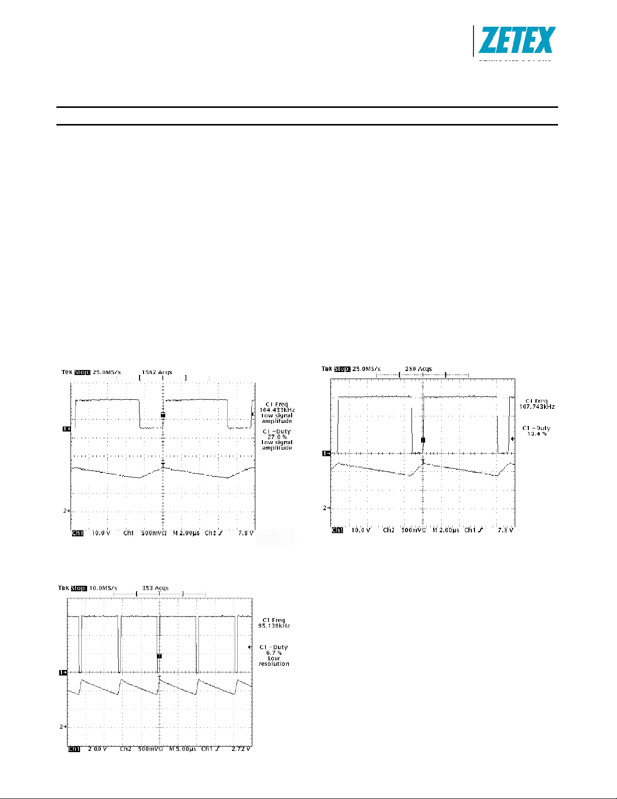
= 15V, RS = 0.1V, L = 100µH Normal operation.
Output Current (Ch1) and LX Voltage (Ch2)
Product Line o
Diodes Incorporated
ZXLD1362
DC or pulse signals to change the V
and adjust the output current.
Details of the different modes of adjusting output current are
given in the applications section.
Output Shutdown
The output of the low pass filter drives the shutdown circuit.
When the input voltage to this circuit falls below the threshold
(0.2V nom.), the internal regulator and the output switch are
turned off. The voltage reference remains powered during
shutdown to provide the bias current for the shutdown circuit.
Quiescent supply current during shutdown is nominally 60A
and switch leakage is below 5A.
V
= 30V, RS = 0.1V, L = 100µH Normal Operation.
IN
Output Current (Ch1) and LX Voltage (Ch2)
switching threshold
SENSE
V
= 60V, RS = 0.1V, L = 100µH Normal Operation.
IN
Output Current (Ch1) and LX Voltage (Ch2)
ZXLD1362
Document number: DS33472 Rev. 5 - 2
6 of 24
www.diodes.com
May 2012
© Diodes Incorporated
Page 7
A
f
D
D
D
D
D
D
y
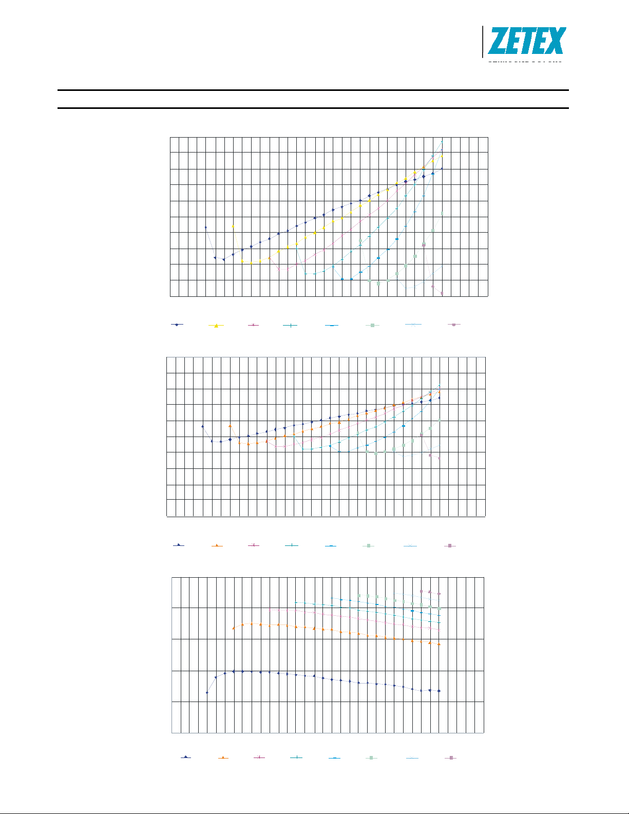
Typical Characteristics
1100
1090
1080
1070
1060
1050
1040
Output Current (mA)
1030
1020
1010
1000
0 7040
1 LED
10%
8%
6%
4%
2%
0%
-2%
-4%
Output Current Deviation
-6%
-8%
-10%
0 7040
1 LED
100%
3 LE
ZXLD1362 Output Current
L = 68µH
Supply Voltage (V)
ZXLD1362 Output Current
L = 68µH
Supply Voltage (V)
7 LED5 LE
ZXLD1362 Efficienc
9 LE
L = 68µH
Product Line o
Diodes Incorporated
13 LE
6010 20 30
15 LED13 LED11 LE D9 LED7 LED5 LED3 LED
6010 20 30
15 LE
50
50
11 LE
ZXLD1362
90%
80%
70%
Efficiency (% )
60%
50%
0 7040
1 LED
ZXLD1362
Document number: DS33472 Rev. 5 - 2
Supply Voltage (V)
7 of 24
www.diodes.com
50
6010 20 30
15 LED13 LED11 LED9 LED7 LED5 LED3 LED
© Diodes Incorporated
May 2012
Page 8
A
f
y
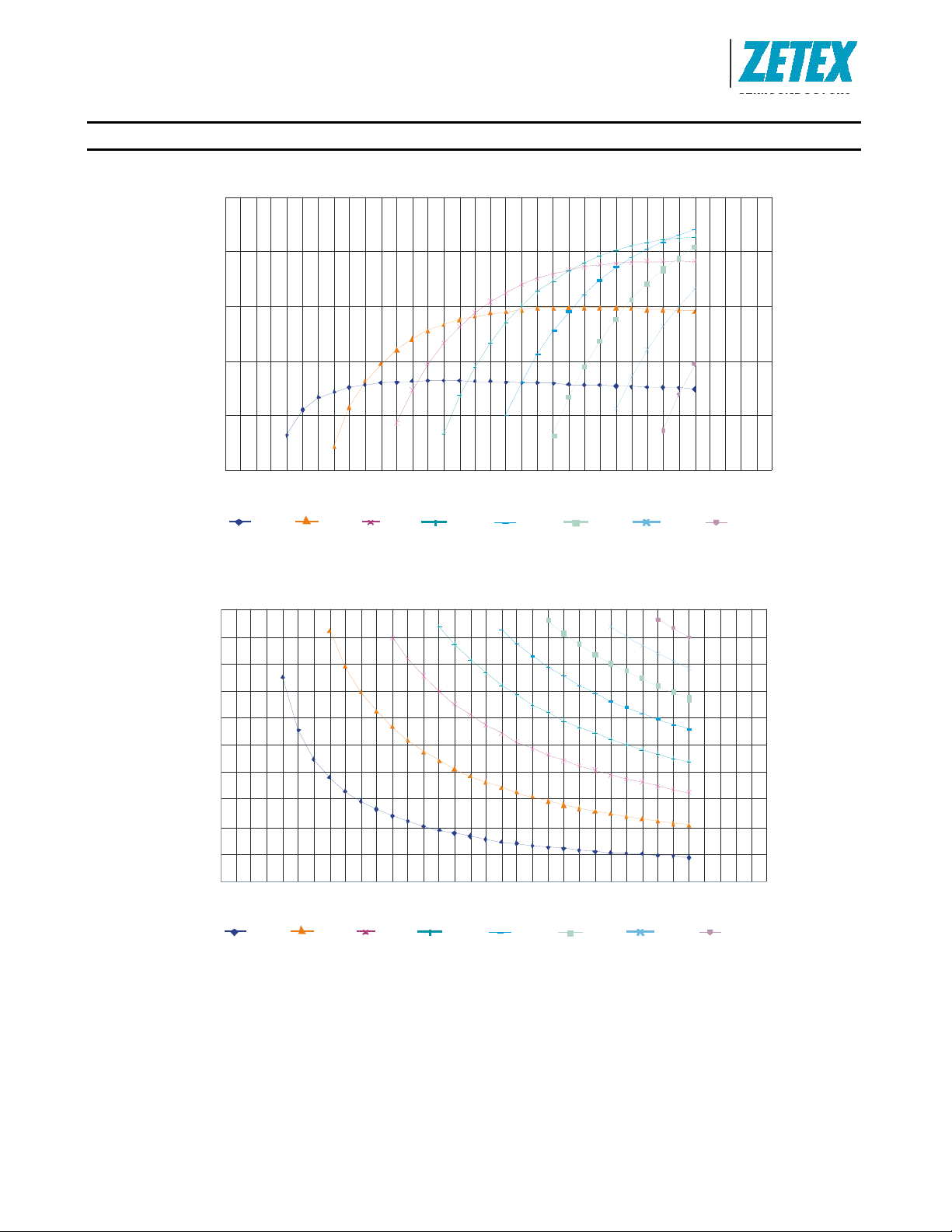
Typical Characteristics (cont.)
500
400
300
200
Switching Frequency (kHz)
100
0
0 7040
1 LED
Diodes Incorporated
ZXLD1362 Switching Frequenc
L = 68µH
Supply Voltage (V)
Product Line o
50
6010 20 30
ZXLD1362
15 LED13 LED11 LE D9 LED7 LED5 LED3 LED
ZXLD1362 Duty Cycle
L = 68µH
100
90
80
70
60
50
40
Du ty Cycle (%)
30
20
10
0
0 7040
1 LED
ZXLD1362
Document number: DS33472 Rev. 5 - 2
Supply Voltage (V)
8 of 24
www.diodes.com
50
6010 20 30
15 LED13 LED11 LED9 LED7 LED5 LED3 LED
May 2012
© Diodes Incorporated
Page 9

A
f
y
Typical Characteristics (cont.)
1100
1090
1080
1070
1060
1050
1040
Output Current (mA)
1030
1020
1010
1000
0 7040
1 LED
10%
8%
6%
4%
2%
0%
-2%
-4%
Output Current Deviation
-6%
-8%
-10%
0 7040
1 LED
100%
ZXLD1362 Output Current
L = 100µH
Supply Voltage (V)
ZXLD1362 Output Current
L = 100µH
Supply Voltage (V)
ZXLD1362 Efficienc
L = 100µH
Product Line o
Diodes Incorporated
50
50
6010 20 30
15 LED13 LED11 LE D9 LED7 LED5 LED3 LED
6010 20 30
15 LED13 LED11 LE D9 LED7 LED5 LED3 LED
ZXLD1362
90%
80%
70%
Efficiency (%)
60%
50%
0 7040
1 LED
ZXLD1362
Document number: DS33472 Rev. 5 - 2
Supply Voltage (V)
9 of 24
www.diodes.com
50
6010 20 30
15 LED13 LED11 LED9 LED7 LED5 LED3 LED
May 2012
© Diodes Incorporated
Page 10

A
f
y
Typical Characteristics (cont.)
500
400
300
200
Switching Frequency (kHz)
100
0
0 7040
1 LED
100
Diodes Incorporated
ZXLD1362 Switching Frequency
L = 100µH
Supply Voltage (V)
ZXLD1362 Switching F requenc
L = 100µH
Product Line o
50
6010 20 30
15 LED13 LED11 LED9 LED7 LED5 LED3 LED
ZXLD1362
90
80
70
60
50
40
Duty Cycle (%)
30
20
10
0
0 7040
Supply Voltage (V)
1 LED
50
6010 20 30
15 LED13 LED11 LED9 LED7 LED5 LED3 LED
ZXLD1362
Document number: DS33472 Rev. 5 - 2
10 of 24
www.diodes.com
May 2012
© Diodes Incorporated
Page 11

A
f
Typical Characteristics (cont.)
1100
1090
1080
1070
1060
1050
1040
Output Current (mA)
1030
1020
1010
1000
0 7040
1 LED
10%
8%
6%
4%
2%
0%
-2%
-4%
Output Current Deviation
-6%
-8%
-10%
0 7040
1 LED
100%
ZXLD1362 Output Current
L = 150µH
Supply Voltage (V)
ZXLD1362 Output Current
L = 150µH
Supply Voltage (V)
ZXLD1362 Efficiency
L = 150µH
Product Line o
Diodes Incorporated
50
50
6010 20 30
15 LED13 LED11 LED9 LED7 LED5 LED3 LED
6010 20 30
15 LED13 LED11 LE D9 LED7 LED5 LED3 LED
ZXLD1362
90%
80%
70%
Efficiency (%)
60%
50%
0 7040
Supply Voltage (V)
1 LED
ZXLD1362
Document number: DS33472 Rev. 5 - 2
11 of 24
www.diodes.com
50
6010 20 30
15 LED13 LED11 LE D9 LED7 LED5 LED3 LED
May 2012
© Diodes Incorporated
Page 12

A
f
y
Typical Characteristics (cont.)
500
400
300
200
Switching Frequency (kHz)
100
0
0 7040
Diodes Incorporated
ZXLD1362 Switching Frequenc
L = 150µH
Supply Voltage (V)
Product Line o
50
6010 20 30
ZXLD1362
1 LED
ZXLD1362 Duty Cycle
100
90
80
70
60
50
40
Duty Cycle (%)
30
20
10
0
0 7040
1 LED
ZXLD1362
Document number: DS33472 Rev. 5 - 2
L = 150µH
Supply Voltage (V)
12 of 24
www.diodes.com
50
6010 20 30
15 LED13 LED11 LE D9 LED7 LED5 LED3 LED
15 LED13 LED11 LE D9 LED7 LED5 LED3 LED
May 2012
© Diodes Incorporated
Page 13

A
f
y
Typical Characteristics (cont.)
1100
1090
1080
1070
1060
1050
1040
Output Current (mA)
1030
1020
1010
1000
0 7040
1 LED
10%
8%
6%
4%
2%
0%
-2%
-4%
Output Current Deviation
-6%
-8%
-10%
0 7040
1 LED
100%
ZXLD1362 Output Current
L = 220µH
Supply Voltage (V)
ZXLD1362 Output Current
L = 220µH
Supply Voltage (V)
ZXLD1362 Efficienc
L = 220µH
Product Line o
Diodes Incorporated
50
50
6010 20 30
15 LED13 LED11 LED9 LED7 LED5 LED3 LED
6010 20 30
15 LED13 LED11 LE D9 LED7 LED5 LED3 LED
ZXLD1362
90%
80%
70%
Effici ency (%)
60%
50%
0 7040
1 LED
ZXLD1362
Document number: DS33472 Rev. 5 - 2
Supply Voltage (V)
13 of 24
www.diodes.com
50
6010 20 30
15 LED13 LED11 LE D9 LED7 LED5 LED3 LED
May 2012
© Diodes Incorporated
Page 14

A
f
Typical Characteristics (cont.)
500
400
300
200
Switching Frequency (kHz)
100
0
0 7040
1 LED
100
Diodes Incorporated
ZXLD1362 Switching Frequency
L = 2200µH
Supply Voltage (V)
ZXLD 1362 Duty Cycle
L = 2200µH
Product Line o
50
6010 20 30
ZXLD1362
15 LED13 LED11 LE D9 LED7 LED5 LED3 LED
90
80
70
60
50
40
Duty Cycle (%)
30
20
10
0
0 7040
1 LED
ZXLD1362
Document number: DS33472 Rev. 5 - 2
Supply Voltage (V)
14 of 24
www.diodes.com
50
6010 20 30
15 LED13 LED11 LE D9 LED7 LED5 LED3 LED
May 2012
© Diodes Incorporated
Page 15

A
f
j
Typical Characteristics (cont.)
1200
1000
800
600
LED Current (mA)
400
200
0
0123
LED Current vsVad
ADJ Pin Voltage (V)
R=100m R=150m R=330m
Product Line o
Diodes Incorporated
ZXLD1362
800
700
600
500
400
300
200
Supply current (mA)
100
0
010203040506070
1.243
1.2425
1.242
1.2415
1.241
1.2405
1.24
1.2395
1.239
ADJ pin voltage (V)
1.2385
1.238
0 102030405060 70
Supply current
Supply voltage (V)
Vref
Supply voltage (V)
90
80
70
60
50
40
30
20
Shutdown current (mA)
10
0
010203040506070
Shutdow n curr ent
Supply voltage (V)
ZXLD1362
Document number: DS33472 Rev. 5 - 2
15 of 24
www.diodes.com
May 2012
© Diodes Incorporated
Page 16

A
f
m
Typical Characteristics (cont.)
1.6
1.4
1.2
1
0.8
0.6
0.4
On-resistance (Ohms)
0.2
0
0 5 10 15 20 25 30 35
Lx on-resistance vs supply voltage
Supply Voltage (V)
Product Line o
Diodes Incorporated
-40C
20C
150C
ZXLD1362
1.262
1.26
1.258
1.256
1.254
1.252
Vadj (V)
1.25
1.248
1.246
1.244
-50 0 50 100 150 200
Temperature (C)
7V
9V
12V
20V
30V
Lx on-resistance vs die temperature
Vadj vs Temperature
1.6
1.4
s)
1.2
1
0.8
0.6
0.4
On-resistance (Oh
0.2
0
-50 0 50 100 150 200
Die Temperature (C)
7V
9V
12V
20V
30V
ZXLD1362
Document number: DS33472 Rev. 5 - 2
16 of 24
www.diodes.com
May 2012
© Diodes Incorporated
Page 17

A
Product Line o
f
Diodes Incorporated
ZXLD1362
Application Information
Setting Nominal Average Output Current with External
Resistor R
The nominal average output current in the LED(s) is determined by
the value of the external current sense resistor (R
between V
I
OUTnom
The table below gives values of nominal average output current for
several preferred values of current setting resistor (R
application circuit shown on page 1:
The above values assume that the ADJ pin is floating and at a
nominal voltage of V
minimum allowed value of sense resistor under these conditions to
maintain switch current below the specified maximum value.
It is possible to use different values of R
from an external voltage. (See next section).
S
and I
IN
and is given by:
SENSE
= 0.1/RS [for RS > 0.1]
RS (Ω)
0.1 1000
0.13 760
0.15 667
REF
Nominal average output
current (mA)
(= 1.25V). Note that RS = 0.1 is the
if the ADJ pin is driven
S
) connected
S
) in the typical
S
Output Current Adjustment by External DC Control
Voltage
The ADJ pin can be driven by an external dc voltage (V
shown, to adjust the output current to a value above or below the
nominal average value defined by R
+
DC
GND
The nominal average output current in this case is given by:
I
= (V
OUTdc
Note that 100% brightness setting corresponds to V
When driving the ADJ pin above 1.25V, R
proportion to prevent I
The input impedance of the ADJ pin is 50k ±25% for voltages
below V
/1.25) x (100mV/RS) [for 0.3< V
ADJ
and 14.2k ±25% for voltages above V
REF
ADJ
exceeding 1A maximum.
OUTdc
.
S
ZXLD1362
GND
S
<2.5V]
ADJ
must be increased in
+100mV.
REF
ZXLD1362
Document number: DS33472 Rev. 5 - 2
), as
ADJ
= V
ADJ
REF
www.diodes.com
Output Current Adjustment by PWM Control
Directly driving ADJ input
A Pulse Width Modulated (PWM) signal with duty cycle D
be applied to the ADJ pin, as shown below, to adjust the output
current to a value above or below the nominal average value set
GND
S
PWM
GND
:
ADJ
ZXLD1362
GND
ADJ
ZXLD1362
GND
3.3k
ADJ
ZXLD1362
GND
© Diodes Incorporated
by resistor R
V
ADJ
0V
Driving the ADJ Input via Open Collector Transistor
The recommended method of driving the ADJ pin and controlling
the amplitude of the PWM waveform is to use a small NPN
switching transistor as shown below:
PWM
This scheme uses the 50k resistor between the ADJ pin and the
internal voltage reference as a pull-up resistor for the external
transistor.
Driving the ADJ Input from a Microcontroller
Another possibility is to drive the device from the open drain output
of a microcontroller. The diagram below shows one method of
doing this:
MCU
.
If the NMOS transistor within the microcontroller has high Gate /
Drain capacitance, this arrangement can inject a negative spike
into ADJ input of the 1362 and cause erratic operation but the
addition of a Schottky clamp diode (cathode to ADJ) to ground and
inclusion of a series resistor (3.3k) will prevent this. See the
section on PWM dimming for more details of the various modes of
control using high frequency and low frequency PWM signals.
17 of 24
can
PWM
May 2012
Page 18

A
f
OFT STAR
T T
Application Information (cont.)
Shutdown Mode
Taking the ADJ pin to a voltage below 0.2V for more than
approximately 100µs will turn off the output and supply current
to a low standby level of 20µA nominal.
Note that the ADJ pin is not a logic input. Taking the ADJ pin to
a voltage above V
100% nominal average value. (See page 18 graphs for details).
16
14
12
10
IME (ms)
8
will increase output current above the
REF
Product Line o
Diodes Incorporated
ZXLD1362
Soft-Start
An external capacitor from the ADJ pin to ground will provide a
soft-start delay, by increasing the time taken for the voltage on
this pin to rise to the turn-on threshold and by slowing down the
rate of rise of the control voltage at the input of the comparator.
Adding capacitance increases this delay by approximately
200µs/nF. The graph to the left shows the variation of soft-start
time for different values of capacitor.
Actual Operating Waveforms [V
= 24V, R
IN
L = 68µH, 22nF on ADJ]
Soft-start operation. Output current (Ch2) and LX voltage (Ch1)
= 0.1Ω,
S
6
4
S
2
0
-2
Soft Start Time vs. Capacitance from
40 60020 80100120
CAPACITANCE (nF)
ADJ Pin to G r ound
VIN Capacitor Selection
A low ESR capacitor should be used for input decoupling, as
the ESR of this capacitor appears in series with the supply
source impedance and lowers overall efficiency. This capacitor
has to supply the relatively high peak current to the coil and
smooth the current ripple on the input supply.
To avoid transients into the IC, the size of the input capacitor
will depend on the V
= 6 to 40V CIN = 2.2F
V
IN
= 40 to 50V CIN = 4.7F
V
IN
V
= 50 to 60V CIN = 10F
IN
When the input voltage is close to the output voltage the input
current increases which puts more demand on the input
capacitor. The minimum value of 2.2F may need to be
increased to 4.7F; higher values will improve performance at
lower input voltages, especially when the source impedance is
ZXLD1362
Document number: DS33472 Rev. 5 - 2
voltage:
IN
18 of 24
www.diodes.com
high. The input capacitor should be placed as close as possible
to the IC.
For maximum stability over temperature and voltage,
capacitors with X7R, X5R, or better dielectric is recommended.
Capacitors with Y5V dielectric are not suitable for decoupling in
this application and should NOT be used.
If higher voltages are used and the C
electrolytic capacitor provide a suitable 1µF ceramic capacitor
is also used and positioned as close the V
possible.
A suitable capacitor would be NACEW100M1006.3x8TR13F.
The following web sites are useful when finding alternatives:
www.murata.com
www.niccomp.com
www.kemet.com
is 10F. This can be an
IN
of the IC as
IN
May 2012
© Diodes Incorporated
Page 19

A
Product Line o
f
A
r
Diodes Incorporated
ZXLD1362
Application Information (cont.)
Inductor Selection
Recommended inductor values for the ZXLD1362 are in the
range 68H to 220H.
Higher values of inductance are recommended at higher
supply voltages in order to minimize errors due to switching
delays, which result in increased ripple and lower efficiency.
Higher values of inductance also result in a smaller change in
output current over the supply voltage range. (see graphs
pages 10 - 17). The inductor should be mounted as close to
the device as possible with low resistance connections to the
LX and V
The chosen coil should have a saturation current higher than
the peak output current and a continuous current rating above
the required mean output current.
Suitable coils for use with the ZXLD1362 may be selected from
the MSS range manufactured by Coilcraft, or the NPIS range
ZXLD1362
Document number: DS33472 Rev. 5 - 2
pins.
IN
16
15
14
13
12
11
10
9
8
7
Numb er of LEDs
6
5
4
3
2
1
0
0 102030405060
ZXLD1362 Minimum Recommended Inducto
l uminiumboard,2%Accuracy, <60°CCaseTemperature
SupplyVoltage (V)
Figure 3. ZXLD1362 Minimum Recommended Inductor
19 of 24
www.diodes.com
manufactured by NIC components. The following websites may
be useful in finding suitable components.
www.coilcraft.com
www.niccomp.com
www.wuerth-elektronik.de
The inductor value should be chosen to maintain operating
duty cycle and switch 'on'/'off' times within the specified limits
over the supply voltage and load current range.
The graph Figure 3 below can be used to select a
recommended inductor based on maintaining the ZXLD1362
case temperature below 60°C. For detailed performance
characteristics for the inductor values 68, 100, 150 and 220H
see graphs on pages 10-17.
May 2012
© Diodes Incorporated
Page 20

A
f
R
Application Information (cont.)
Diode Selection
For maximum efficiency and performance, the rectifier (D1)
should be a fast low capacitance Schottky diode* with low
reverse leakage at the maximum operating voltage and
temperature.
They also provide better efficiency than silicon diodes, due to a
combination of lower forward voltage and reduced recovery
time.
It is important to select parts with a peak current rating above
the peak coil current and a continuous current rating higher
than the maximum output load current. It is very important to
consider the reverse leakage of the diode when operating
above +85°C. Excess leakage will increase the power
V
IN
s
Product Line o
Diodes Incorporated
ZXLD1362
dissipation in the device and if close to the load may create a
thermal runaway condition.
The higher forward voltage and overshoot due to reverse
recovery time in silicon diodes will increase the peak voltage
on the LX output. If a silicon diode is used, care should be
taken to ensure that the total voltage appearing on the LX pin
including supply ripple, does not exceed the specified
maximum value.
*A suitable Schottky diode would be 30BQ100PBF (IR).
Reducing Output Ripple
Peak to peak ripple current in the LED(s) can be reduced, if
required, by shunting a capacitor Cled across the LED(s) as
shown below:
D1
V
IN
I
ZXLD1362
A value of 1F will reduce the supply ripple current by a factor
three (approx.). Proportionally lower ripple can be achieved
with higher capacitor values. Note that the capacitor will not
affect operating frequency or efficiency, but it will increase
start-up delay, by reducing the rate of rise of LED voltage.
By adding this capacitor the current waveform through the
LED(s) changes from a triangular ramp to a more sinusoidal
version without altering the mean current value.
Operation at Low Supply Voltage
Below the under-voltage lockout threshold (VSD) the drive to
the output transistor is turned off to prevent device operation
SENSE
CledLED
L1
LX
with excessive on-resistance of the output transistor. The
output transistor is not full enhanced until the supply voltage
exceeds approximately 17V. At supply voltages between V
and 17V care must be taken to avoid excessive power
dissipation due to the on-resistance.
If the supply voltage is always less than 30V continuous an
alternative device is available, the ZXLD1360 or the AL8805.
Note that when driving loads of two or more LEDs, the forward
drop will normally be sufficient to prevent the device from
switching below approximately 6V. This will minimize the risk of
damage to the device.
SD
ZXLD1362
Document number: DS33472 Rev. 5 - 2
20 of 24
www.diodes.com
May 2012
© Diodes Incorporated
Page 21

A
Product Line o
f
P
O
R
Diodes Incorporated
ZXLD1362
Application Information (cont.)
Thermal Considerations
When operating the device at high ambient temperatures, or
when driving maximum load current, care must be taken to
avoid exceeding the package power dissipation limits. The
Note that the device power dissipation will most often be a
maximum at minimum supply voltage. It will also increase if the
efficiency of the circuit is low. This may result from the use of
unsuitable coils, or excessive parasitic output capacitance on
the switch output.
1100
1000
900
800
700
(mW)
600
500
WE
400
300
200
100
0
-10 10-50 -30 30 90 110
AMBIENT TEMPERATURE (°C)
Maximum Power Dissipation
Thermal Compensation of Output Current
High luminance LEDs often need to be supplied with a
temperature compensated current in order to maintain stable
and reliable operation at all drive levels. The LEDs are usually
mounted remotely from the device so, for this reason, the
temperature coefficients of the internal circuits for the
ZXLD1362 have been optimized to minimize the change in
output current when no compensation is employed. If output
current compensation is required, it is possible to use an
external temperature sensing network - normally using
Negative Temperature Coefficient (NTC) thermistors and/or
diodes, mounted very close to the LED(s). The output of the
sensing network can be used to drive the ADJ pin in order to
reduce output current with increasing temperature.
ZXLD1362
Document number: DS33472 Rev. 5 - 2
21 of 24
www.diodes.com
graph below gives details for power derating. This assumes the
device to be mounted on a 25mm
standing in still air.
130 15050 70
2
PCB with 1oz copper
Layout Considerations
LX Pin
The LX pin of the device is a fast switching node, so PCB
tracks should be kept as short as possible. To minimize ground
'bounce', the ground pin of the device should be soldered
directly to the ground plane.
Coil and Decoupling Capacitors and Current Sense
Resistor
It is particularly important to mount the coil and the input
decoupling capacitor as close to the device pins as possible to
minimize parasitic resistance and inductance, which will
degrade efficiency. It is also important to minimize any track
resistance in series with current sense resistor R
connect V
opposite end of R
tracks. It is important that the cathode current of the Schottky
diode does not flow in a track between R
give an apparent higher measure of current than is actual
because of track resistance.
directly to one end of RS and I
IN
with no other currents flowing in these
S
and VIN as this may
S
. Its best to
S
directly to the
SENSE
May 2012
© Diodes Incorporated
Page 22

A
Product Line o
f
Diodes Incorporated
ZXLD1362
Application Information (cont.)
ADJ Pin
The ADJ pin is a high impedance input for voltages up to 1.35V
so, when left floating, PCB tracks to this pin should be as short as
possible to reduce noise pickup. A 100nF capacitor from the ADJ
pin to ground will reduce frequency modulation of the output
under these conditions. An additional series 3.3k resistor can
also be used when driving the ADJ pin from an external circuit
(see below). This resistor will provide filtering for low frequency
noise and provide protection against high voltage transients.
3.3k
100nF
ADJ
ZXLD1362
GND
GND
High Voltage Tracks
Avoid running any high voltage tracks close to the ADJ pin, to
reduce the risk of leakage currents due to board contamination.
The ADJ pin is soft-clamped for voltages above 1.35V to
desensitize it to leakage that might raise the ADJ pin voltage and
cause excessive output current. However, a ground ring placed
around the ADJ pin is recommended to minimize changes in
output current under these conditions.
Evaluation PCB
ZXLD1362 evaluation boards are available on request and
provide quick testing of the ZXLD1362 device.
ZXLD1362
Document number: DS33472 Rev. 5 - 2
22 of 24
www.diodes.com
Dimming Output Current Using PWM
Low Frequency PWM Mode
When the ADJ pin is driven with a low frequency PWM signal
(eg 100Hz), with a high level voltage V
zero, the output of the internal low pass filter will swing
between 0V and V
to fall below its turn-off threshold (200mV nom) when the ADJ
pin is low. This will cause the output current to be switched on
and off at the PWM frequency, resulting in an average output
current I
OUTavg
(See Figure 4 - Low frequency PWM operating waveforms).
Figure 4. Low Frequency PWM Operating Waveforms
The average value of output current in this mode is given by:
I
= 0.1D
OUTavg
This mode is preferable if optimum LED 'whiteness' is required.
It will also provide the widest possible dimming range (approx.
1000:1) and higher efficiency at the expense of greater output
ripple.
, causing the input to the shutdown circuit
ADJ
proportional to the PWM duty cycle.
PWM/RS
[for D
PWM
>0.001]
and a low level of
ADJ
May 2012
© Diodes Incorporated
Page 23

A
Product Line o
f
A
θ
Diodes Incorporated
ZXLD1362
Ordering Information
Device Part Mark
ZXLD1362ET5TA 1362 ET5 TSOT25 180 8 3000 TA 1
Note: 11. Pad layout as shown on Diodes Inc. suggested pad layout document AP02001, which can be found on our website at
http://www.diodes.com/datasheets/ap02001.pdf.
Package
Code
Packaging
(Note 11)
Reel size
(mm)
Reel width
(mm)
Quantity
per reel
Part Number
Suffix
AEC-Q100
grade
Package Outline Dimensions
TSOT25
E1
A2
A
1
D
e1
e
5x b
E
L2
4x 1
θ
c
L
TSOT25
Dim Min Max Typ
A
A1 0.01 0.10
A2 0.84 0.90
D
E
E1
b 0.30 0.45
c 0.12 0.20
e
e1
L 0.30 0.50
L2
θ 0° 8° 4°
θ1 4° 12°
All Dimensions in mm
1.00
−
− −
− −
− −
− −
− −
− −
−
−
−
2.90
2.80
1.60
−
−
0.95
1.90
0.25
−
Suggested Pad Layout
TSOT25
ZXLD1362
Document number: DS33472 Rev. 5 - 2
Y1
C C
X (5x)
Y (5x)
23 of 24
www.diodes.com
Dimensions Value (in mm)
C
X
Y
Y1
0.950
0.700
1.000
3.199
May 2012
© Diodes Incorporated
Page 24

A
Product Line o
f
Diodes Incorporated
ZXLD1362
DIODES INCORPORATED MAKES NO WARRANTY OF ANY KIND, EXPRESS OR IMPLIED, WITH REGARDS TO THIS DOCUMENT,
INCLUDING, BUT NOT LIMITED TO, THE IMPLIED WARRANTIES OF MERCHANTABILITY AND FITNESS FOR A PARTICULAR
PURPOSE (AND THEIR EQUIVALENTS UNDER THE LAWS OF ANY JURISDICTION).
Diodes Incorporated and its subsidiaries reserve the right to make modifications, enhancements, improvements, corrections or other changes
without further notice to this document and any product described herein. Diodes Incorporated does not assume any liability arising out of the
application or use of this document or any product described herein; neither does Diodes Incorporated convey any license under its patent or
trademark rights, nor the rights of others. Any Customer or user of this document or products des cribed herein in such applications shall
assume all risks of such use and will agree to hold Diodes Incorporated and all the companies whose products are represented on Diodes
Incorporated website, harmless against all damages.
Diodes Incorporated does not warrant or accept any liability whatsoever in respect of any products purchased through unauthorized sales
channel.
Should Customers purchase or use Diodes Incorporated products for any unintended or unauthorized application, Customers shall indemnify
and hold Diodes Incorporated and its representatives harmless against all claims, damages, expenses, and attorney fees arising out of,
directly or indirectly, any claim of personal injury or death associated with such unintended or unauthorized application.
Products described herein may be covered by one or more United States, international or foreign patents pending. Product names and
markings noted herein may also be covered by one or more United States, international or foreign trademarks.
Diodes Incorporated products are specifically not authorized for use as critical components in life support devices or systems without the
express written approval of the Chief Executive Officer of Diodes Incorporated. As used herein:
A. Life support devices or systems are devices or systems which:
1. are intended to implant into the body, or
2. support or sustain life and whose failure to perform when properly used in accordance with instructions for use provided in the
labeling can be reasonably expected to result in significant injury to the user.
B. A critical component is any component in a life support device or system whose failure to perform can be reasonably expected to cause
the failure of the life support device or to affect its safety or effectiveness.
Customers represent that they have all necessary expertise in the safety and regulatory ramifications of their life support devices or systems,
and acknowledge and agree that they are solely responsible for all legal, regulatory and safety-related requirements concerning their products
and any use of Diodes Incorporated products in such safety-critical, life support devices or systems, notwithstanding any devices- or systemsrelated information or support that may be provided by Diodes Incorporated. Further, Customers must fully indemnify Diodes Incorporated and
its representatives against any damages arising out of the use of Diodes Incorporated products in such safety-critical, life support devices or
systems.
Copyright © 2012, Diodes Incorporated
IMPORTANT NOTICE
LIFE SUPPORT
www.diodes.com
ZXLD1362
Document number: DS33472 Rev. 5 - 2
24 of 24
www.diodes.com
May 2012
© Diodes Incorporated
 Loading...