Diodes ZXLD1360 User Manual
A
Product Line o
f
Diodes Incorporated
ZXLD1360
30V 1A LED DRIVER with AEC-Q100
Description
The ZXLD1360 is a continuous mode inductive step-down
converter with integrated switch and high side current sense.
It operates from an input supply from 7V to 30V driving single
or multiple series connected LEDs efficiently externally
adjustable output current up to 1mA.
The ZXLD1360 has been qualified to AEC-Q100 Grade 1
enabling operation in ambient temperatures from -40°C to
125°C.
The output current can be adjusted by applyi ng a DC voltage
or a PWM waveform to the ADJ pin; 100:1 adjustment of
output current is possible using PWM control. Applying
0.2V or lower to the ADJ pin turns the output off and switches
the device into a low current standby state.
Features
• Simple low parts count
• Single pin on/off and brightness control using DC voltage
or PWM
• High efficiency (up to 95%)
• Wide input voltage range: 7V to 30V
• 40V transient capability
• Qualified to AEC-Q100 Grade 1
• Available in thermally enhanced packages
o TSOT23-5 θ
• Available in Green molding (no Br, Sb) with lead free
finish/RoHS compliant
• Up to 1MHz switching frequency
• Typical 4% output current accuracy
JA
82° C/W
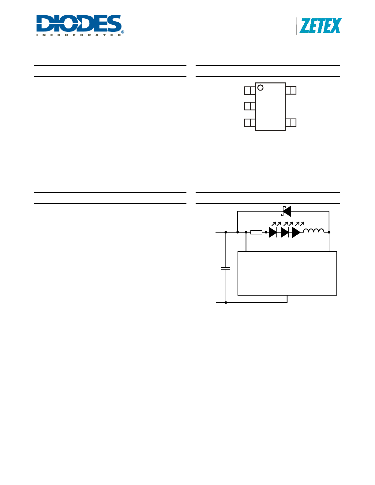
Pin Assignments
LX
GND
ADJ
TSOT23-5
Top Vi ew
Typical Application Circuit
R
R
S
V
V
ADJ
ADJ
0.1Ω
0.1Ω
IN
IN
S
SET
SET
ZXLD1360
ZXLD1360
GND
GND
VIN`
VIN`
7~30V
7~30V
C1
C1
4.7µF
4.7µF
GND
GND
V
IN
I
SENSE
L1
L1
47µH
47µH
LX
LX
ZXLD1360
Document number: DS33471 Rev. 4 - 2
1 of 25
www.diodes.com
March 2011
© Diodes Incorporated
A
f
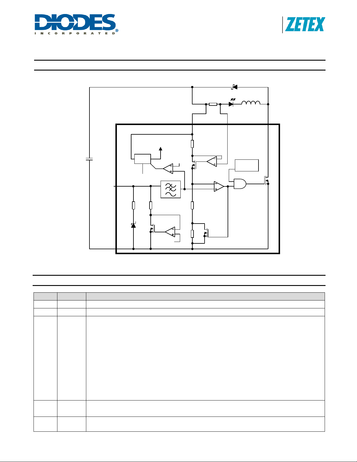
Block Diagram
Product Line o
Diodes Incorporated
ZXLD1360
D1
V
IN
C1
4.7µF
ADJ
Voltage
regulator
5V
R
S
V
54 1
IN
R1
0.2V
SENSE
L1
``
Low voltage
detector
LXI
MN
3
R5
R4
200k
1.25V
GND
20k
D1
1.35V
2
R2
R3
Figure 1. Block diagram – With Pin Connections
Pin Descriptions
Name Pin No. Description
LX 1 Drain of NDMOS switch
GND 2 Ground (0V)
Multi-function On/Off and brightness control pin:
• Leave floating for normal operation.(V
o I
OUTnom
= 0.1/RS)
• Drive to voltage below 0.2V to turn off output current
ADJ 3
• Drive with DC voltage (0.3V < V
OUTnom
I
ADJ
• Drive with PWM signal from open-collector or open-drain transistor, to adjust output current.
• Adjustment range 25% to 100% of I
500Hz
• Connect a capacitor from this pin to ground to increase soft-start time.
(Default soft-start time = 500µs. Additional soft-start time is approximately 500µs/nF)
I
SENSE
VIN
4
5
ZXLD1360
Document number: DS33471 Rev. 4 - 2
Connect resistor RS from this to VIN to define nominal average output current I
(Note: R
=0.1V with ADJ pin open circuit)
SMIN
Input voltage (7V to 30V). Decouple to ground with 4.7µF of higher X7R ceramic capacitor close to
device
2 of 25
www.diodes.com
ADJ
= V
= 1.25V giving nominal average output current
REF
< 2.5V) to adjust output current from 25% to 200% of
for f>10kHz and 1% to 100% of I
OUTnom
OUTnom
OUTnom
=0.1/RS
for f <
© Diodes Incorporated
March 2011
A
Product Line o
f
Diodes Incorporated
ZXLD1360
Absolute Maximum Ratings (Voltages to GND Unless Otherwise Stated)
Symbol Parameter Rating Unit
VIN
V
SENSE
VLX
V
ADJ
ILX
P
TOT
TST
TJ
MAX
These are stress ratings only. Operation above the absolute maximum rating may cause device failure. Operation at the absolute maximum ratings, for extended
periods, may reduce device reliability.
Input Voltage
I
SENSE
Voltage
LX Output Voltage
Adjust Pin Input Voltage -0.3 to +6 V
Switch Output Current 1.25 A
Power Dissipation
(Refer to Package thermal de-rating curve on page 20)
Storage Temperature -55 to 150 °C
Junction Temperature 150 °C
ESD Susceptibility
Rating Unit
Human Body Model 500 V
Machine Model <100 V
Semiconductor devices are ESD sensitive and may be damaged by exposure to ESD events. Suitable ESD precautions should be taken when handling and
transporting these devices.
The human body model is a 100pF capacitor discharge through a 1.5k resistor pin. The machine model is a 200pF capacitor discharged directly into each pin
-0.3 to +30
(40V for 0.5 sec)
+0.3 to -5
(measured with respect to VIN)
-0.3 to +30
(40V for 0.5 sec)
1 W
V
V
V
Thermal Resistance
Symbol Parameter Rating Unit
θ
JA
JB
Junction to Ambient 82
°C/W
Junction to Board 33 °C/W
Recommended Operating Conditions
Symbol Parameter Min Max Units
VIN
ILX
V
ADJ
V
ADJoff
t
ONmin_REC
f
LX max
DLX
TA
Notes: 1. ZXLD1360 will operate at higher frequencies but due to propagation delays accuracy will be affected.
2.100% brightness corresponds to V
current proportionally.
Input Voltage Range 7 30 V
Maximum recommended continuous/RMS switch current 1 A
External control voltage range on ADJ pin for DC brightness
control (Note 2)
DC voltage on ADJ pin to ensure devices is off 0.25 V
Recommended minimum switch “ON” time 800 ns
Recommended maximum operating frequency (Note 1) 625 kHz
0.3 2.5 V
Duty cycle range 0.01 0.99
Ambient operating temperature range -40 125 °C
ADJ
= V
ADJ(nom)
= V
(~1.25V). Driving the ADJ pin above V
REF
will increase the V
REF
SENSE
threshold and output
ZXLD1360
Document number: DS33471 Rev. 4 - 2
3 of 25
www.diodes.com
March 2011
© Diodes Incorporated

A
Product Line o
f
Diodes Incorporated
ZXLD1360
Electrical Characteristics (Test conditions: V
= 12V, TA = 25°C, unless otherwise specified. Note 3)
IN
Symbol Parameter Condition Min. Typ. Max. Unit
VSU
VSD
I
INQoff
I
INQon
V
SENSE
V
SENSEHYS
I
SENSE
V
REF
ΔV
REF
V
ADJ
V
ADJoff
V
ADJon
R
ADJ
I
LXmean
RLX
I
LX(leak)
Internal regulator start-up threshold
Internal regulator shutdown threshold
Quiescent supply current with output off ADJ pin grounded 20 40 µA
Quiescent supply current with output switching
Mean current sense threshold voltage
(Defines LED current setting accuracy)
Sense threshold hysteresis ±15 %
I
pin input current V
SENSE
Internal reference voltage
/ΔT Temperature coefficient of V
External control voltage range on ADJ pin for DC
brightness control (Note 2)
DC voltage on ADJ pin to switch device from
active (on) state to quiescent (off) state
DC voltage on ADJ pin to switch device from
quiescent (off) state to active (on) state
Resistance between ADJ pin and V
Continuous LX switch current 1 A
LX switch ‘On’ resistance
LX switch leakage current 5 µA
Duty cycle range of PWM signal applied to ADJ
D
PWM(LF)
pin during low frequency PWM dimming mode
Brightness control range 100:1
Duty cycle range of PWM signal applied to ADJ
D
PWM(HF)
pin during high frequency PWM dimming mode
Brightness control range 5:1
REF
REF
VIN rising
VIN falling
ADJ pin floating
f=250kHz
Measured on I
with respect to V
= 1.25V
V
ADJ
SENSE
SENSE
= VIN-0.1
IN
Measured on ADJ pin
with pin floating
pin
5.65 V
5.55 V
1.8 5.0 mA
95 100 105 mV
1.25 10 µA
1.25 V
50 ppm/°C
0.3 2.5 V
falling
V
ADJ
rising
V
ADJ
0 < V
V
ADJ
ADJ
> V
< V
REF
+100mV
REF
@ ILX=0.55A
PWM frequency <500Hz
PWM amplitude = V
REF
0.15 0.2 0.25 V
0.2 0.25 0.3 V
135
13.5
250
25
0.5 1.0
0.01 1
Measured on ADJ pin
PWM frequency >10kHz
PWM amplitude = V
REF
0.16 1
Measured on ADJ pin
Time taken for output
current to reach 90% of
final value after voltage
on ADJ pin has risen
500 µs
tSS
Soft start time
above 0.3V
ADJ pin floating
fLX
Operating frequency
(See graphs for more details)
L = 33µH (0.093V)
= 1A @ V
I
OUT
LED
= 3.6V
280 kHz
Driving 1 LED
t
OFFMIN
t
ONMIN
tPD
Notes: 3. Production testing of the device is performed at 25°C. Functional operation of the device and parameters spe cifi ed over a -40°C to +125°C
temperature range, are guaranteed by design, characterization and process control.
Minimum switch off-time 200 ns
Minimum switch on-time 240 ns
Internal comparator propagation delay 50 ns
k
ZXLD1360
Document number: DS33471 Rev. 4 - 2
4 of 25
www.diodes.com
March 2011
© Diodes Incorporated

A
Product Line o
f
Diodes Incorporated
ZXLD1360
Device Description
The device, in conjunction with the coil (L1) and current sense resistor (RS), forms a self-oscillating continuous-mode buck
converter.
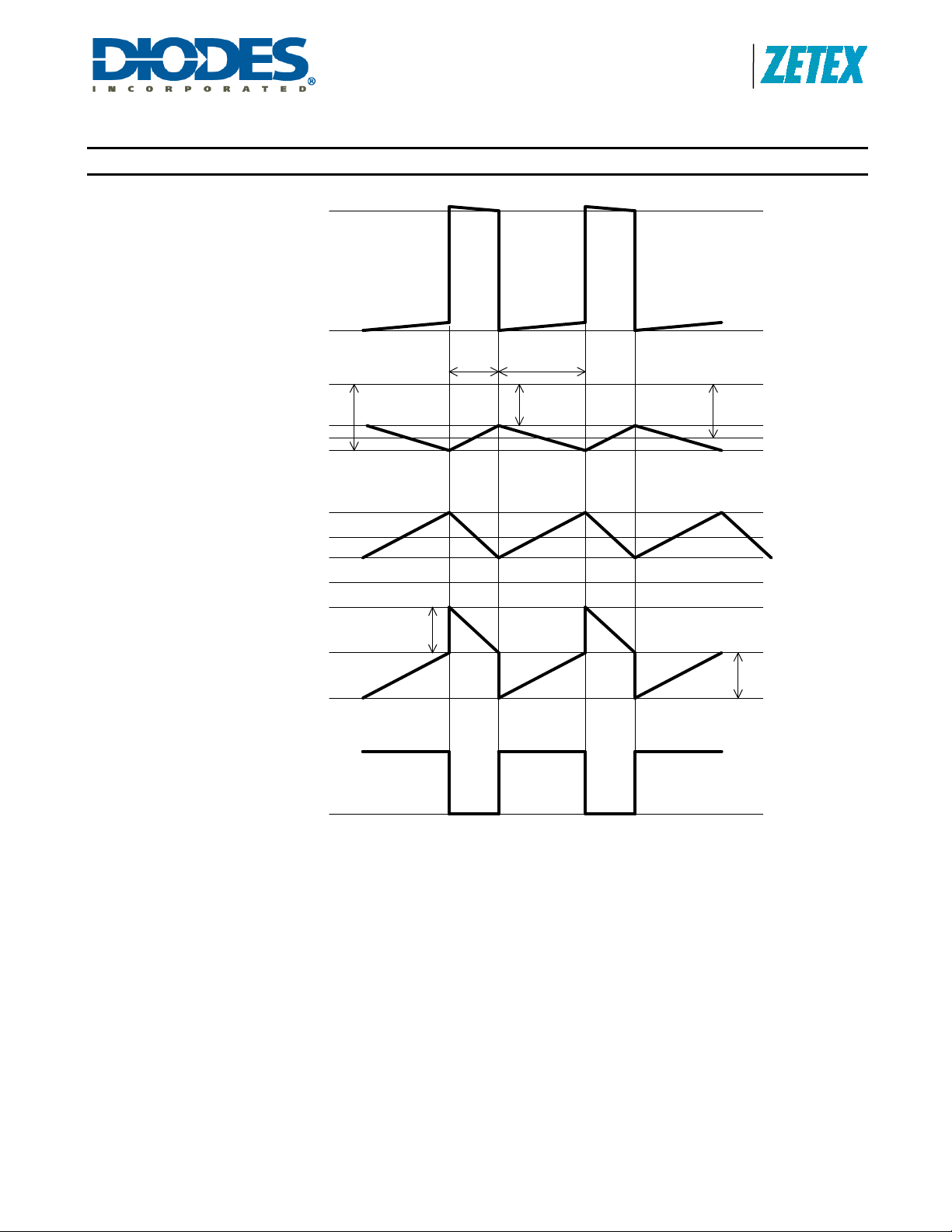
Device operation (refer to Figure 1 - Block diagram and Figure 2 Operating waveforms)
Operation can be best understood by assuming that the ADJ pin of the device is unconnected and the voltage on this pin
(VADJ) appears directly at the (+) input of the comparator.
When input voltage V
circuit. Under this condition, the (-) input to the comparator is at ground and its output is high. This turns MN on and switches
the LX pin low, causing current to flow from V
by VIN and L1 to produce a voltage ramp (V
resistor R1 by the current sense circuit and produces a proportional current in internal resistors R2 and R3. T his produces a
ground referred rising voltage at the (-) input of the comparator. When this reaches the threshold voltage (V
comparator output switches low and MN turns off. The comparator output also drives another NMOS switch, which bypasses
internal resistor R3 to provide a controlled amount of hysteresis. The hysteresis is set by R3 to be nominally 15% of V
When MN is off, the current in L1 continues to flow via D1 and the LED(s) back to V
determined by the LED(s) and diode forward voltages to produce a falling voltage at the input of the co mparator. When this
voltage returns to V
ramping between limits of V
Switching thresholds
With V
I
SENSE
I
OUTnom
Nominal ripple current is ±15mV/RS
= V
ADJ
REF
pin with respect to VIN). The average output current I
= 100mV/RS
Adjusting output current
The device contains a low pass filter between the ADJ pin and the threshold comparator and an internal current limiting
resistor (200kV nom) between ADJ and the internal reference voltage. T his allows the ADJ pin to be overdriven with either
DC or pulse signals to change the V
comprising three sections, each with a cut-off frequency of nominally 4kHz.
Details of the different modes of adjusting output current are given in the applications section.
Output shutdown
The output of the low pass filter drives the shutdo wn circuit. When the input voltage to this circuit falls below the threshold
(0.2V nom.), the internal regulator and the output switch are turned off. The voltage reference remains powered during
shutdown to provide the bias current for the shutdown circuit. Quiesce nt supply current during shutdown is nominally 20mA
and switch leakage is below 5mA.
ZXLD1360
Document number: DS33471 Rev. 4 - 2
is first applied, the initial current in L1 and RS is zero and there is no output from the current sense
IN
to ground, via RS, L1 and the LED(s). The current rises at a rate determined
IN
) across RS. The supply referred voltage V
SENSE
IN
, the comparator output switches high again. This cycle of events repeats, with the comparator inpu t
ADJ
± 15%.
ADJ
, the ratios of R1, R2 and R3 define an average V
is then defined by this voltage and RS according to:
OUTnom
switching threshold and adjust the output current. The filter is third order,
SENSE
5 of 25
www.diodes.com
switching threshold of 100mV (measured on the
SENSE
is forced across internal
SENSE
. The current decays at a rate
© Diodes Incorporated
), the
ADJ
.
ADJ
March 2011
A
f
Device Description
Product Line o
Diodes Incorporated
ZXLD1360
SENSE voltage
Coil current
Comparator
input voltage
Comparator
output
LX voltage
V
IN
0V
V
IN
0V
0.15V
ADJ
V
ADJ
5V
0V
Toff Ton
85mV
100mV115mV
V
SENSE-
V
SENSE+
0.15V
I
OUTnom
I
OUTnom
I
OUTnom
ADJ
+15%
-15%
Figure 2. Operating Waveforms
ZXLD1360
Document number: DS33471 Rev. 4 - 2
6 of 25
www.diodes.com
March 2011
© Diodes Incorporated
A
Product Line o
f
Diodes Incorporated
ZXLD1360
Device Description (cont.)
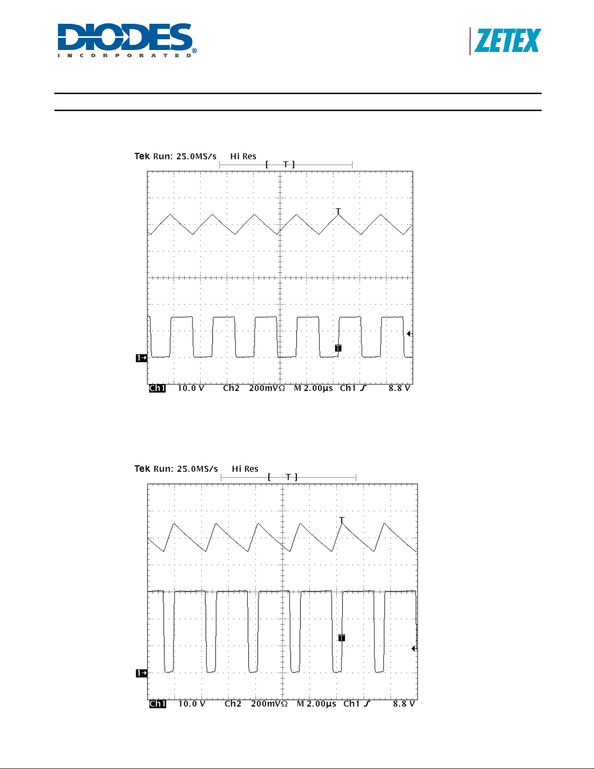
Actual operating waveforms [VIN=15V, RS=0.1V, L=33µH]
Normal operation. Output current (Ch1) and LX voltage (Ch2)
Actual operating waveforms [V
Normal operation. Output current (Ch1) and LX voltage (Ch2)
ZXLD1360
Document number: DS33471 Rev. 4 - 2
=30V, RS=0.1V, L=33µH]
IN
7 of 25
www.diodes.com
March 2011
© Diodes Incorporated
A
f
y
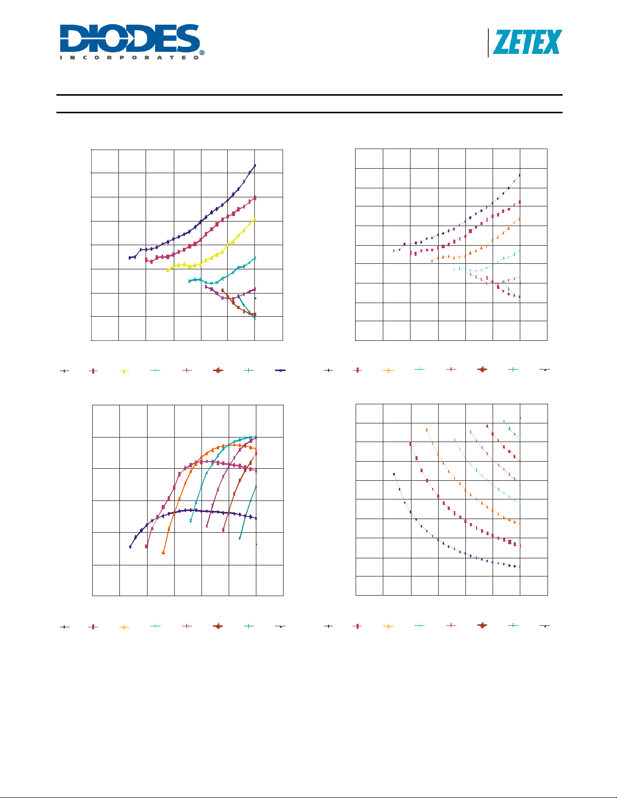
Typical Operating Characteristics
Product Line o
Diodes Incorporated
ZXLD1360
1060
1040
1020
1000
980
960
Output Current (mA)
940
920
900
0 510
600
500
ZXLD1360 Output Current
ZXLD1360 Switching Frequenc
L = 33µH
15
20 25 30 35
Supply Voltage V (V)
L = 33µH
IN
5 LEDs4 LEDs3 LEDs2 LEDs1 LED
10%
8%
6%
4%
2%
0%
-2%
-4%
Output Current Deviation (%)
-6%
-8%
-10%
0 510
8 LEDs7 LEDs6 LEDs
100
90
80
ZXLD1360 Output Current
L = 33µH
15
20 25 30 35
Supply Voltage V (V)
ZXLD1360 Duty Cycle
L = 33µH
IN
5 LEDs4 LEDs3 LEDs2 LEDs1 LED
8 LEDs7 LEDs6 LEDs
400
300
200
Switching Frequency (kHz)
100
0
0 510
15
20 25 30 35
Supply Voltage V (V)
IN
5 LEDs4 LEDs3 LED s2 LEDs1 LED
8 LEDs7 LEDs6 LEDs
70
60
50
40
Duty Cycle (%)
30
20
10
0
0 510
15
20 25 30 35
Supply Voltage V (V)
IN
5 LEDs4 LEDs3 LEDs2 LEDs1 LED
8 LEDs7 LEDs6 LEDs
ZXLD1360
Document number: DS33471 Rev. 4 - 2
8 of 25
www.diodes.com
March 2011
© Diodes Incorporated
 Loading...