
A
f
Product Line o
Diodes Incorporated
ZXLD1356/ ZXLD1356Q
60V 550mA LED DRIVER and AUTOMOTIVE GRADE
Description
The ZXLD1356 is a continuous mode inductive step-down converter,
designed for driving single or multiple series connected LEDs efficiently
from a voltage source higher than the LED voltage. The device operates
from an input supply between 6V and 60V and provides an externally
adjustable output current of up to 550mA. Depending upon supply
voltage and external components, this can provide up to 30 watts of
output power.
The ZXLD1356 has been qualified to AECQ100 Grade 1 enabling
operation in ambient temperatures from -40°C to +125°C
Output current can be adjusted above, or below the set value, by
applying an external control signal to the 'ADJ' pin. Enhanced output
current dimming can be achieved by applying a PWM signal to the ‘ADJ’
pin.
Features
• Typically better than 0.8% output current accuracy
• Simple and with low part count
• Single pin on/off and brightness control using DC voltage or PWM
• PWM resolution up to 1000:1
• High efficiency (up to 97%)
• Wide input voltage range: 6V to 60V
• Inherent open-circuit LED protection
• Available in thermally enhanced packages
V-DFN3030-6 θ
TSOT25 θ
• Available in “Green” Molding Compound (No Br, Sb) with lead Free
Finish/ RoHS Compliant
Totally Lead-Free & Fully RoHS Compliant (Notes 1 & 2)
Halogen and Antimony Free. “Green” Device (Note 3)
• ZXLD1356QET5TA Automotive Grade qualified to AEC-Q100
Grade 1
Notes: 1. No purposely added lead. Fully EU Directive 2002/95/EC (RoHS) & 2011/65/EU (RoHS 2) compliant.
2. See http://www.diodes.com for more information about Diodes Incorporated’s definitions of Halogen and Antimony free, "Green" and Lead-Free.
3. Halogen and Antimony free "Green” products are defined as those which contain <900ppm bromine, <900ppm chlorine (<1500ppm total Br + Cl)
and <1000ppm antimony compounds.
JA
JA
ZXLD1356/ ZXLD1356Q
Document number: DS33470 Rev. 4 - 2
44°C/W
82°C/W
www.diodes.com
Pin Assignments
(TOP VIEW)
1
LX
2
GND
3
ADJ
(TOP VIEW)
LX
1
2
GND
34
ADJ
V-DFN3030-6
Applications
• Low Voltage Halogen Replacement LEDs
• Automotive Lighting
• Low Voltage Industrial Lighting
• LED Back-Up Lighting
• Illuminated Signs
• Emergency Lighting
• SELV Lighting
• Refrigeration Lights
1 of 29
TSOT25
6
5
5
4
V
GND
I
SENSE
V
IN
I
SENSE
IN
October 2012
© Diodes Incorporated
A
f
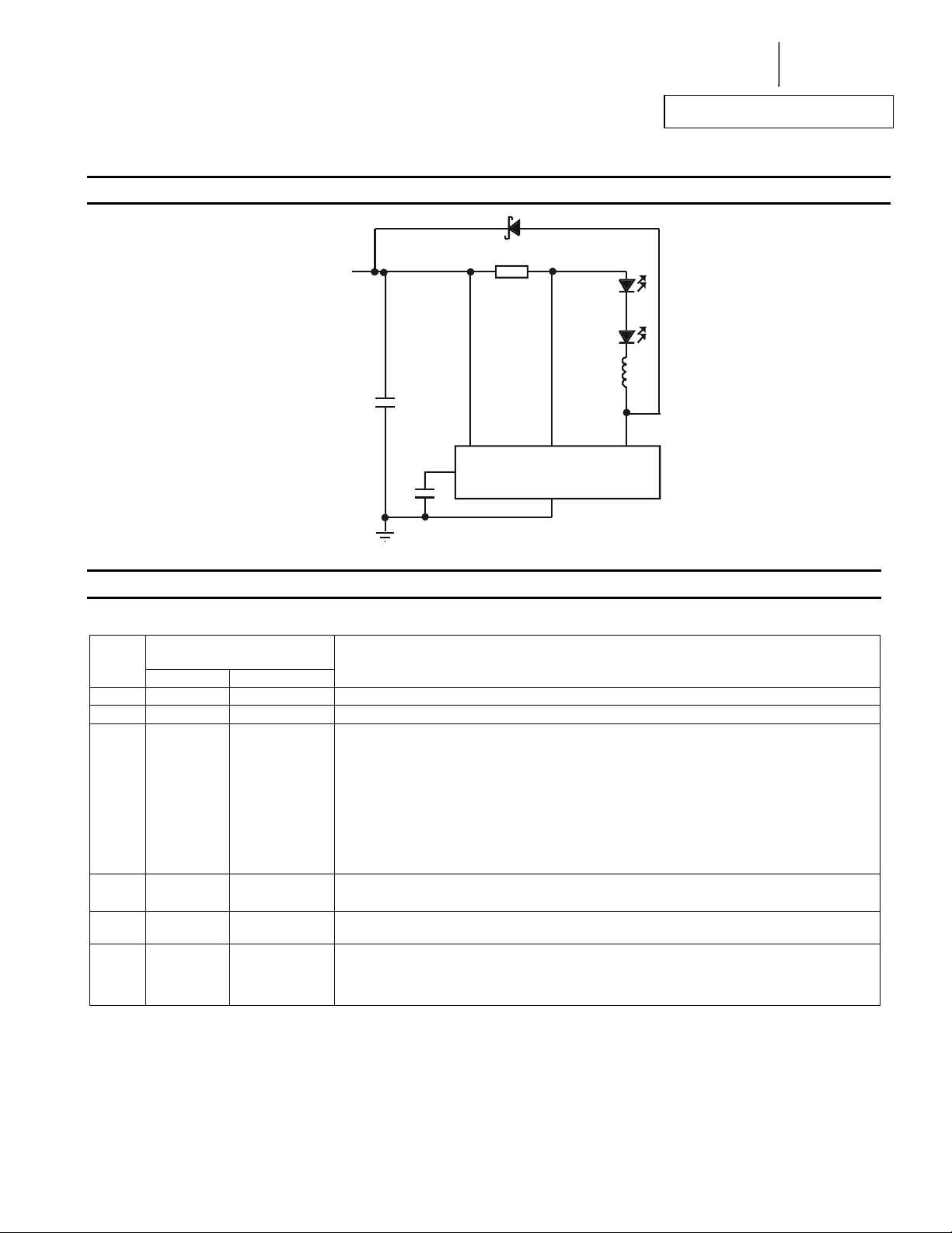
Typical Applications Circuit
Product Line o
Diodes Incorporated
ZXLD1356/ ZXLD1356Q
D1
VIN(24V)
Rs
0.36V
L1
4.7µFC1
100nF
V
ADJ
IN
I
SENSE
ZXLD1356
GND
LX
GND
Pin Descriptions
Pin
Name
LX 1 1 Drain of NDMOS switch
GND 2 2, 5 Ground (0V)
ADJ 3 3
I
SENSE
VIN
Pad — Pad
TSOT25 V-DFN3030-6
ZXLD1356/ ZXLD1356Q
Document number: DS33470 Rev. 4 - 2
Pin
Number
Multi-function On/Off and brightness control pin:
• Leave floating for normal operation.(V
• Drive to voltage below 0.2V to turn off output current
• Drive with DC voltage (0.3V<V
• Connect a capacitor from this pin to ground to define soft-start time.
4 4
5 6
Connect resistor R
(Note: R
Input voltage (6V to 60V). Decouple to ground with 4.7µF of higher X7R ceramic capacitor close
to device
Exposed pad (EP) - connected to device substrate.
To improve thermal impedance of package the EP must be connected to power ground but
should not be used as the 0V (GND) current path.
It can be left floating but must not be connected to any other voltage other than 0V.
current
o I
I
OUTnom
Soft-start time is approx.0.2ms/nF
SMIN
= 0.2V/RS)
OUTnom
ADJ
from this to VIN to define nominal average output current I
S
=0.36V with ADJ pin open circuit)
2 of 29
www.diodes.com
Function
= V
ADJ
<2.5V) to adjust output current from 24% to 200% of
= 1.25V giving nominal average output
REF
= 0.2/RS
OUTnom
October 2012
© Diodes Incorporated
A
f
V
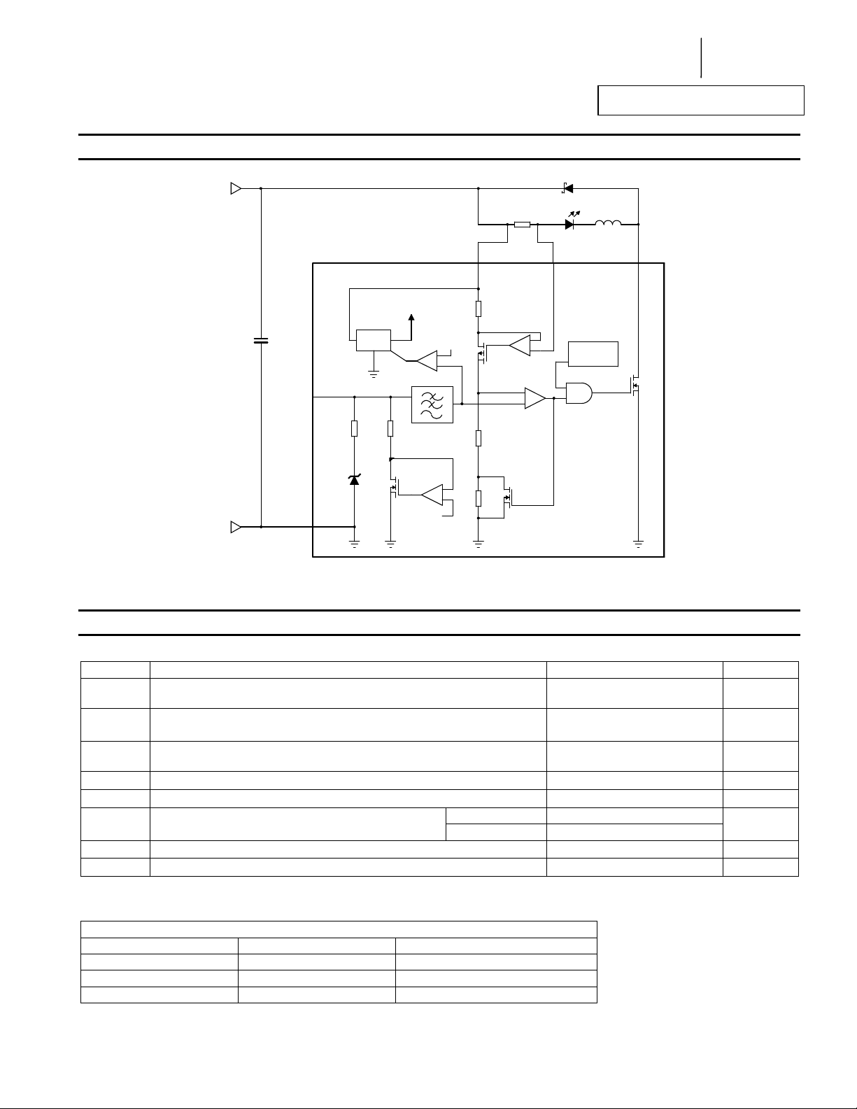
Functional Block Diagram
IN
Product Line o
Diodes Incorporated
ZXLD1356/ ZXLD1356Q
R
D1
S
L1
I
SENSE
-
+
-
+
Low voltage
detector
LX
MN
C1
4.7μF
Gnd
Adj
V
54 1
IN
Voltage
regulator
5V
R1
0.2V
-
+
3
R5
50K
1.25V
R4
20K
D1
600KHz
1.35V
R2
-
+
R3
2
Figure 1. Block Diagram – Pin Connections Shown for TSOT25 Package
Absolute Maximum Ratings (Voltages to GND, unless otherwise specified.)
Symbol Parameter Rating Unit
VIN
V
SENSE
VLX
V
ILX
P
TOT
TST
TJ
These are stress ratings only. Operation outside the absolute maximum ratings may cause device failure.
Operation at the absolute maximum rating for extended periods may reduce device reliability.
Input Voltage
I
SENSE
Voltage
(measured with respect to V
LX Output Voltage
Adjust Pin Input Voltage -0.3 to +6.0 V
ADJ
Switch Output Current 0.65 A
Power Dissipation
(Refer to package thermal de-rating curve on page 25)
TSOT25 1
V-DFN3030-6 1.8
Storage Temperature -55 to +150 °C
Junction Temperature 150 °C
MAX
ESD Susceptibility
Rating Unit
Human Body Model 500 V
Charged Device Model >1000 V
Machine Model <100 V
Semiconductor devices are ESD sensitive and may be damaged by exposure to ESD events. Suitable ESD precautions should be taken when handling and
transporting these devices.
The human body model is a 100pF capacitor discharge through a 1.5k resistor pin. The machine model is a 200pF capacitor discharged directly into each pin.
ZXLD1356/ ZXLD1356Q
Document number: DS33470 Rev. 4 - 2
3 of 29
www.diodes.com
-0.3 to +60
(65V for 0.5 sec)
+0.3 to -5.0
-0.3 to +60
(65V for 0.5 sec)
)
IN
W
October 2012
© Diodes Incorporated
V
V
V
A
f
Product Line o
Diodes Incorporated
ZXLD1356/ ZXLD1356Q
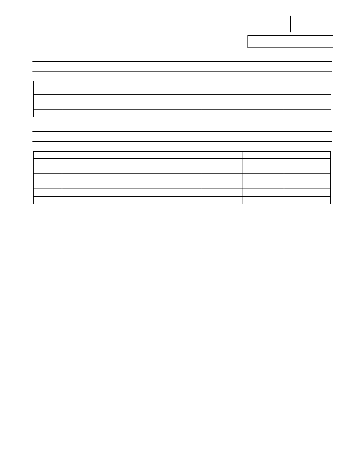
Thermal Resistance
Symbol Parameter
Recommended Operating Conditions (@T
Symbol Parameter Min Max Units
VIN
t
OFFMIN
t
ONMIN
f
LX max
DLX
TOP
Notes: 4. VIN > 16V to fully enhance output transistor. Otherwise out current must be derated - see graphs. Operation at low supply may cause excessive heating
due to increased on-resistance. Tested at 7V guaranteed for 6V by design.
5. ZXLD1356 will operate at higher frequencies but accuracy will be affected due to propagation delays.
ZXLD1356/ ZXLD1356Q
Document number: DS33470 Rev. 4 - 2
Junction to Ambient 82
JA
Junction to Board 33
JB
Junction to Case —
JC
= +25°C, unless otherwise specified.)
A
Input voltage (Note 4) 6 60 V
Minimum switch off-time 800 ns
Minimum switch on-time 800 ns
Recommended maximum operating frequency (Note 5) 625 kHz
Duty cycle range 0.01 0.99
Operating temperature range -40 +125 °C
4 of 29
www.diodes.com
TSOT25 V-DFN3030-6
Rating Unit
44
—
14
°C/W
°C/W
°C/W
October 2012
© Diodes Incorporated

A
f
Product Line o
Diodes Incorporated
ZXLD1356/ ZXLD1356Q
Electrical Characteristics (V
Symbol Parameter Condition Min Typ Max Unit
VSU
VSD
I
INQoff
I
INQon
V
SENSE
V
SENSEHYS
I
SENSE
V
REF
ΔV
REF
V
ADJ
V
ADJoff
V
ADJon
R
ADJ
I
LXmean
RLX
I
LX(leak)
D
PWM(LF)
DC
ADJ
tSS
fLX
f
LXmax
Notes: 6. Static current of device is approximately 700 µA, see Graph, Page 17.
7. 100% brightness corresponds to V
proportionally.
8. Ratio of maximum brightness to minimum brightness before shutdown V
Internal regulator start-up threshold 4.85 5.2 V
Internal regulator shutdown threshold 4.40 4.75 V
Quiescent supply current with output off ADJ pin grounded 65 108 µA
Quiescent supply current with output switching
(Note 6)
Mean current sense threshold voltage
(Defines LED current setting accuracy)
Sense threshold hysteresis ±15 %
I
pin input current V
SENSE
Internal reference voltage
/ΔT Temperature coefficient of V
External control voltage range on ADJ pin for
DC brightness control (Note 7)
DC voltage on ADJ pin to switch device from
active (on) state to quiescent (off) state
DC voltage on ADJ pin to switch device from
quiescent (off) state to active (on) state
Resistance between ADJ pin and V
Continuous LX switch current 0.55 A
LX switch ‘On’ resistance
LX switch leakage current 5 µA
Duty cycle range of PWM signal applied to ADJ
pin during low frequency PWM dimming mode
Brightness control range 1000:1
(*)
DC Brightness control range Note 8 5:1
Start up time
(See graphs for more details)
Operating frequency
(See graphs for more details)
Recommended maximum operating frequency 500 kHz
= 24V, @T
IN
REF
= V
ADJ
AMB
0< V
REF
= V
ADJ(nom)
= +25°C, unless otherwise specified.)
ADJ pin floating, L = 68mH,
3 LEDsf = 360kHz
Measured on I
to V
SENSE
IN VADJ
= V
= 1.25V; V
IN
pin with respect
SENSE
-0.2
= 18V
IN
Measured on ADJ pin with pin
floating
1.6 mA
195 200 205 mV
4 10 µA
1.25 V
50 ppm/°C
0.3 2.5 V
V
falling
ADJ
V
rising
ADJ
< V
, V
> V
+100mV
REF
@ I
ADJ
= 0.55A
LX
REF
ADJ
PWM frequency <300Hz PWM
amplitude = V
REF
0.15 0.20 0.27 V
0.2 0.25 0.3 V
30
10.4
50
14.2
65
18.0
k
0.5 0.75
0.001 1
Measured on ADJ pin
Time taken for output current to reach
90% of final value after voltage on
ADJ pin has risen above 0.3V.
2 ms
Requires external capacitor 22nF.
ADJ pin floating L= 68mH (0.36V)
= 0.55A @ V
I
OUT
LED
= 3.6V
360 kHz
Driving 3 LEDs
. Driving the ADJ pin above V
REF
=1.25/0.25. V
REF
will increase the V
REF
externally driven to 2.5V, ratio 10.1.
REF
SENSE
. threshold and output current
ZXLD1356/ ZXLD1356Q
Document number: DS33470 Rev. 4 - 2
5 of 29
www.diodes.com
October 2012
© Diodes Incorporated
A
f
Product Line o
Diodes Incorporated
ZXLD1356/ ZXLD1356Q
Device Description
The device, in conjunction with the coil (L1) and current sense resistor (RS), forms a self-oscillating continuous-mode buck converter.
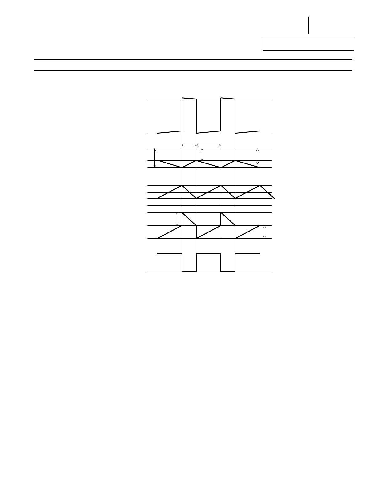
Device operation (refer to Figure 1 - Block diagram and Figure 2 operating waveforms)
LX voltage
V
IN
SENSE voltage
Coil current
Comparator
input voltage
Comparator
output
0V
V
IN
0V
0.15V
ADJ
V
ADJ
5V
0V
Toff Ton
170mV
200mV230mV
V
SENSE-
V
SENSE+
I
+15%
OUTnom
I
OUTnom
-15%
I
OUTnom
0.15V
ADJ
Operation can be best understood by assuming that the ADJ pin of the device is unconnected and the voltage on this pin (V
at the (+) input of the comparator.
When input voltage V
is first applied, the initial current in L1 and RS is zero and there is no output from the current sense circuit. Under this
IN
condition, the (-) input to the comparator is at ground and its output is high. This turns MN on and switches the LX pin low, causing current to flow
from V
to ground, via RS, L1 and the LED(s). The current rises at a rate determined by VIN and L1 to produce a voltage ramp (V
IN
. The supply referred voltage V
R
S
is forced across internal resistor R1 by the current sense circuit and produces a proportional current in
SENSE
internal resistors R2 and R3. This produces a ground referred rising voltage at the (-) input of the comparator. When this reaches the threshold
voltage (V
), the comparator output switches low and MN turns off. The comparator output also drives another NM OS switch, which bypasses
ADJ
internal resistor R3 to provide a controlled amount of hysteresis. The hysteresis is set by R3 to be nominally 15% of V
When MN is off, the current in L1 continues to flow via D1 and the LED(s) back to V
and diode forward voltages to produce a falling voltage at the input of the comparator. When this voltage returns to V
switches high again. This cycle of events repeats, with the comparator input ramping between limits of V
Switching Thresholds
With V
to V
I
OUTnom
Nominal ripple current is ±30mV/R
= V
ADJ
). The average output current I
IN
= 200mV/R
, the ratios of R1, R2 and R3 define an average V
REF
S
OUTnom
S
ZXLD1356/ ZXLD1356Q
Document number: DS33470 Rev. 4 - 2
Figure 2. Theoretical Operating Waveforms
. The current decays at a rate determined by the LED(s)
IN
switching threshold of 200mV (measured on the I
SENSE
is then defined by this voltage and RS according to:
6 of 29
www.diodes.com
ADJ
± 15%.
) appears directly
ADJ
SENSE
.
ADJ
, the comparator output
ADJ
pin with respect
SENSE
October 2012
© Diodes Incorporated
) across

A
f
Product Line o
Diodes Incorporated
ZXLD1356/ ZXLD1356Q
Device Description (cont.)
Adjusting Output Current
The device contains a low pass filter between the ADJ pin and the threshold comparator and an internal current limiting resistor (50k nom)
between ADJ and the internal reference voltage. This allows the ADJ pin to be overdriven with either DC or pulse signals to change the V
switching threshold and adjust the output current.
Details of the different modes of adjusting output current are given in the applications section.
Output Shutdown
The output of the low pass filter drives the shutdown circuit. When the input voltage to this circuit falls below the threshold (0.2V nom.), the
internal regulator and the output switch are turned off. The voltage reference remains powered during shutdown to provide the bias current for
the shutdown circuit. Quiescent supply current during shutdown is nominally 60µA and switch leakage is below 5µA.
ZXLD1356/ ZXLD1356Q
Document number: DS33470 Rev. 4 - 2
www.diodes.com
7 of 29
October 2012
© Diodes Incorporated
SENSE
A
f
Product Line o
Diodes Incorporated
ZXLD1356/ ZXLD1356Q
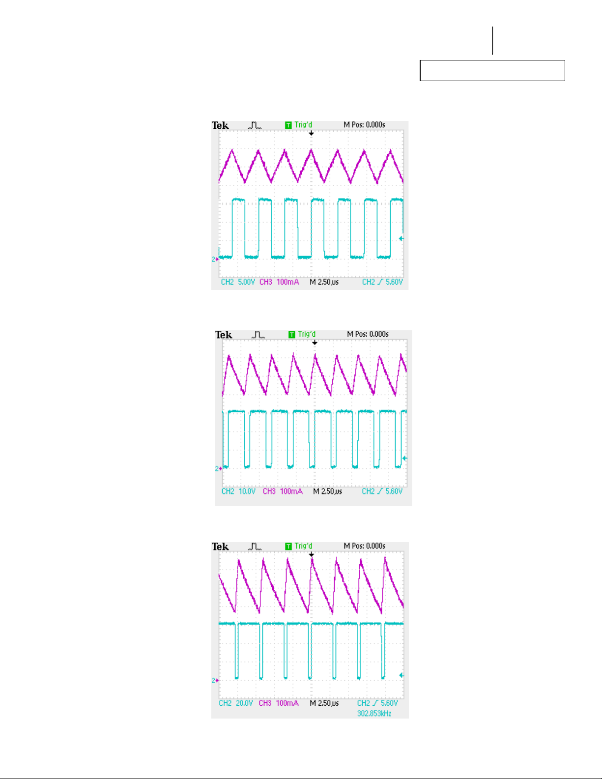
Actual Operating Waveforms [V
Normal operation. Output current (Ch3) and LX voltage (Ch2)
Actual Operating Waveforms [V
Normal operation. Output current (Ch3) and LX voltage (Ch2)
Actual Operating Waveforms [V
Normal operation. Output current (Ch3) and LX voltage (Ch2)
ZXLD1356/ ZXLD1356Q
Document number: DS33470 Rev. 4 - 2
= 15V, RS = 0.36V, L = 68µH]
IN
= 30V, RS = 0.36V, L = 68µH]
IN
= 60V, RS = 0.36V, L = 68µH]
IN
www.diodes.com
8 of 29
October 2012
© Diodes Incorporated
A
f
y
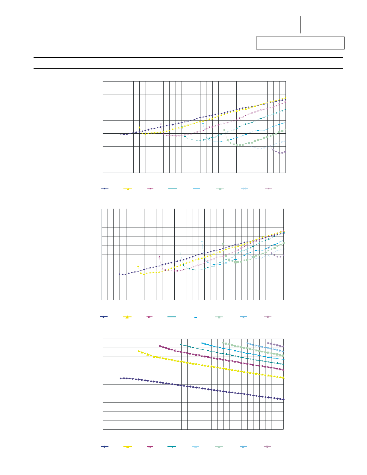
Typical Operating Conditions
0.640
0.620
0.600
0.580
0.560
Outp ut Current (A)
0.540
0.520
0.500
040
1 LED
ZXLD1 356 Output Current
L = 68µH
Supply Voltage (V)
Product Line o
Diodes Incorporated
ZXLD1356/ ZXLD1356Q
50
6010 20 30
15 LEDs13 LEDs11 LEDs9 LEDs7 LEDs5 LEDs3 LEDs
ZXLD1356 Output Current Deviation (Normalized)
10%
8%
6%
4%
2%
0%
-2%
-4%
Output Current Deviation (%)
-6%
-8%
-10%
040
1 LED
100%
95%
90%
85%
80%
75%
70%
Effici ency (%)
65%
60%
55%
50%
040
1 LED
ZXLD1356/ ZXLD1356Q
Document number: DS33470 Rev. 4 - 2
L = 68µH
Supply Voltage (V)
ZXLD1356 Efficienc
L = 68µH
Supply Voltage (V)
9 of 29
www.diodes.com
50
50
6010 20 30
15 LEDs13 LEDs11 LE Ds9 LEDs7 LEDs5 LEDs3 LEDs
6010 20 30
15 LEDs13 LEDs11 LEDs9 LEDs7 LEDs5 LEDs3 LEDs
October 2012
© Diodes Incorporated
 Loading...