Diodes ZXLD1352 User Manual
A Product Line o
f
Diodes Incorporated
ZXLD1352
30V 350mA LED DRIVER WITH 1000:1 PWM DIMMING AND AEC-Q100
Description
The ZXLD1352 is a continuous mode inductive step-down
converter with integrated switch and high side current sense.
It operates from an input supply from 7V to 30V driving
single and multiple series connected LEDs effciently
externally adjustable output current up to 350mA.
The ZXLD1352 has been qualified to AEC-Q100 Grade
2 allowing it to operate at ambient temperatures from -40 to
105°C.
DC voltage or a PWM waveform. 1000:1 adjustment of
output current is possible using PWM control. Applying a
voltage of 0.2V or lower to the ADJ pin turns the output off
and switches the device into a low current standby state.
Features
• Simple low parts count
• Single pin on/off and brightness control using DC voltage
or PWM
• 1000:1 PWM dimming range
• High efficiency (up to 95%)*
• Wide input voltage range: 7V to 30V
• 40V transient capability
• Up to 1MHz switching frequency
• Typical 4% output current accuracy
• Qualified to AEC-Q100 Grade 2
• Available in Green molding (no Br, Sb) with lead free
finish/RoHS compliant
Applications
• Low voltage halogen replacement LEDs
• Automotive lighting
• Low voltage industrial lighting
• LED back-up lighting
• Illuminated signs
* Using standard external components as specified under electrical characteristics. Efficiency is dependent upon the number of LEDs driven and on external
component types and values.
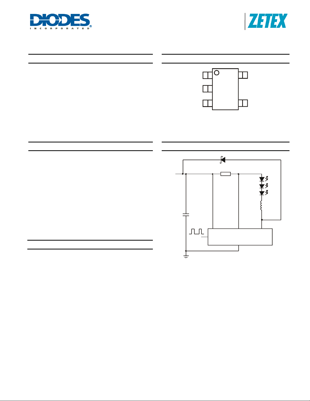
Pin Assignments
LX
GND
ADJ
TSOT23-5
Top View
Typical Application Circuit
V
IN
(12V- 30V)
C1
GND
1µF
PW M
V
ADJ
IN
ZLLS1000
Rs
0.33
D1
I
SENSE
ZXLD1352
GND
V
IN
I
SENSE
47mHL1
LX
ZXLD1352
Document number: DS33469 Rev. 3 - 2
1 of 21
www.diodes.com
December 2010
© Diodes Incorporated
f
V
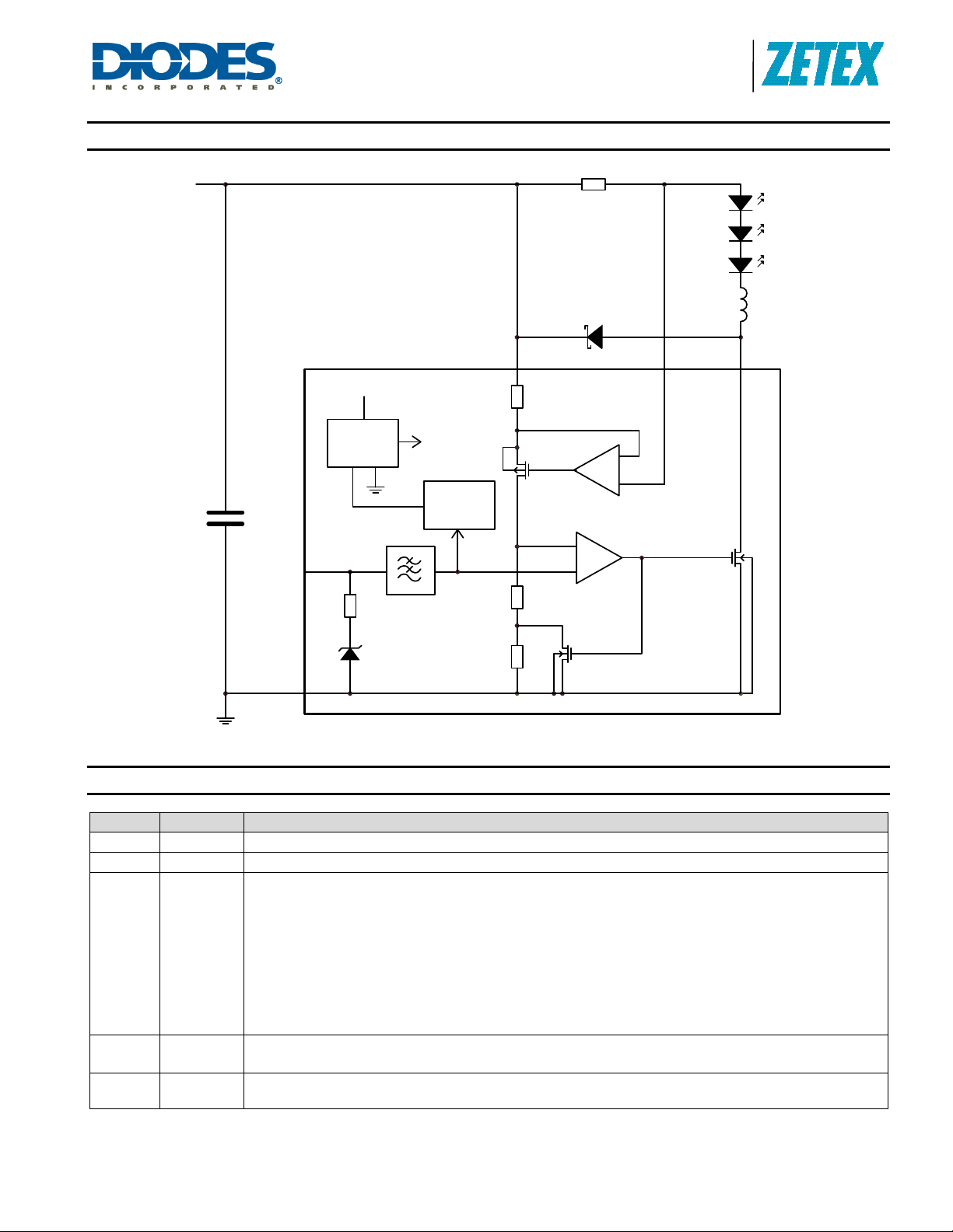
Block Diagram
IN
C1
ADJ
GND
Vref
V
IN
Voltage
regulator
50k
1.25V
V
IN
R1
Current sense circuit
5V
Shutdown
circuit
600KHz
R2
R3
Figure 1. Block Diagram
A Product Line o
Diodes Incorporated
R
S
D1
I
SENSE
-
+
Comparator
-
+
ZXLD1352
L1
LX
MN
Pin Description
Name Pin No. Description
LX 1 Drain of NDMOS switch
GND 2 Ground (0V)
Multi-function On/Off and brightness control pin:
• Leave floating for normal operation. (V
=0.1/RS)
I
OUTnom
• Drive to voltage below 0.2V to turn off output current
ADJ 3
• Drive with DC voltage (0.3V<V
<2.5V) to adjust output current from 25% to 200%† of I
ADJ
• Drive with PWM signal from open-collector or open-drain transistor, to adjust output current.
o Adjustment range 0.1% to 100% of I
• Connect a capacitor from this pin to ground to define soft-start time. Soft-start time is
approx.0.5ms/nF)
I
4
SENSE
VIN 5
Connect resistor R
(Note: R
=0.27V with ADJ pin open circuit)
SMIN
Input voltage (7V to 30V). Decouple to ground with 1µF of higher X7R ceramic capacitor close to
device
ZXLD1352
Document number: DS33469 Rev. 3 - 2
from this to VIN to define nominal average output current I
S
2 of 21
www.diodes.com
= V
ADJ
OUTnom
=1.25V giving nominal average output current
REF
for 100Hz < f < 1kHz
OUTnom
=0.1/RS
December 2010
© Diodes Incorporated
OUTnom
A Product Line o
f
Diodes Incorporated
ZXLD1352
Absolute Maximum Ratings (Voltages to GND Unless Otherwise Stated)
Symbol Parameter Rating Unit
VIN
V
SENSE
VLX
V
ADJ
ILX
P
TOT
TST
TJ
These are stress ratings only. Operation above the absolute maximum rating may cause device failure. Operation at the absolute maximum ratings, for extended
periods, may reduce device reliability.
Input Voltage
I
SENSE
Voltage
LX Output Voltage
Adjust Pin Input Voltage -0.3 to +6 V
Switch Output Current 500 mA
Power Dissipation
(Refer to Package thermal de-rating curve on page 17)
Storage Temperature -55 to 150 °C
Junction Temperature 150 °C
MAX
-0.3 to +30
(40V for 0.5 sec)
+0.3 to -5
(measured with respect to VIN)
-0.3 to +30
(40V for 0.5 sec)
450 mW
V
V
V
Thermal Resistance
Symbol Parameter Rating Unit
θ
Junction to Ambient 200 °C/W
JA
Recommended Operating Conditions
Symbol Parameter Min Max Units
VIN
t
OFFMIN
t
ONMIN
f
LXmax
DLX
TA
ZXLD1352
Document number: DS33469 Rev. 3 - 2
Input voltage 7 30 V
Minimum switch off-time 200 ns
Minimum switch on-time 200 ns
Recommended maximum operating frequency 1 MHz
Duty cycle range 0.01 0.99
Ambient Temperature range -40 105
3 of 21
www.diodes.com
December 2010
© Diodes Incorporated
°C

A Product Line o
f
)
Diodes Incorporated
ZXLD1352
Electrical Characteristics (Test conditions: V
Symbol
Parameter Conditions Min. Typ. Max.
VSU Internal regulator start-up threshold V
I
INQoff
I
INQon
V
SENSE
V
SENSEHYS
I
SENSE
V
Internal reference voltage Measured on ADJ pin with pin floating 1.21 1.25 1.29 V
REF
ΔV
REF
V
ADJ
Quiescent supply current
with output off
Quiescent supply current
with output switching
Mean current sense threshold voltage
(defines LED current setting accuracy)
Sense threshold hysteresis ±15 %
I
/ΔT
pin input current V
SENSE
Temperature coefficient of V
External control voltage range on ADJ
pin for dc brightness control
50 ppm/°C
REF
1
= 12V, T
IN
rising 4.8 V
IN
= 25°C, unless otherwise specified.)
amb
ADJ pin grounded 20 30 µA
ADJ pin floating
f = 250kHz
Measured on I
to V
SENSE
=1.25V
IN VADJ
= VIN -0.1 1.25 10 µA
pin with respect
SENSE
250 500 µA
95 100 105 mV
0.3 2.5 V
DC voltage on ADJ pin to switch device
V
ADJoff
from active (on) state to quiescent (off)
V
falling 0.15 0.2 0.25 V
ADJ
state
DC voltage on ADJ pin to switch device
V
ADJon
from quiescent (off) state to active (on)
V
rising 0.2 0.25 0.3 V
ADJ
state
Unit
R
Resistance between ADJ pin and V
ADJ
I
Continuous LX switch current 0.37 A
LXmean
35 65 kΩ
REF
RLX LX Switch ‘On’ resistance 1.5 2 Ω
I
LX switch leakage current 1 µA
LX(leak
D
PWM(LF)
Duty cycle range of PWM signal
applied to ADJ pin during PWM
dimming mode
PWM frequency 100Hz – 1kHz
PWM amplitude = V
REF
Measured on ADJ pin
0.001 1
Brightness control range 1000:1
ADJ pin floating
fLX
Operating frequency
(See graphs for more detail)
L=100µH (0.82V)
=350mA @ V
I
OUT
LED
=3.4V
250 kHz
Driving 1 LED
tPD Internal comparator propagation delay 50 ns
Notes: 1. Production testing of the device is performed at 25°C. Functional operation of the device and parameters specified over a -40°C to +105°C temperature
range, are guaranteed by design, characterization and process control.
2. 100% brightness corresponds to V
proportionally.
ADJ
= V
ADJ(nom)
= V
. Driving the ADJ pin above V
REF
will increase the V
REF
threshold and output current
SENSE
ZXLD1352
Document number: DS33469 Rev. 3 - 2
4 of 21
www.diodes.com
December 2010
© Diodes Incorporated

A Product Line o
f
Diodes Incorporated
ZXLD1352
Device Description
The device, in conjunction with the coil (L1) and current sense resistor (RS), forms a self-oscillating continuous-mode buck
converter
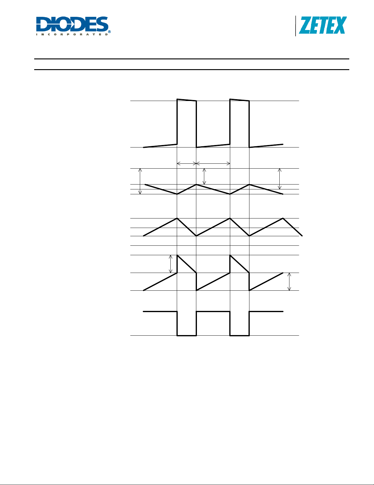
Device operation (Refer to block diagram and Figure 1 - Operating waveforms)
Operation can be best understood by assuming that the ADJ pin of the device is unconnected and the voltage on this pin (V
appears directly at the (+) input of the comparator.
ADJ
)
When input voltage V
is first applied, the initial current in L1 and RS is zero and there is no output from the current sens e
IN
circuit. Under this condition, the (-) input to the comparator is at ground and its output is high. This turns MN on and switches the
LX pin low, causing current to flow from V
and L1 to produce a voltage ramp (V
to ground, via RS, L1 and the LED(s). The current rises at a rate determined by VIN
IN
) across RS. The supply referred voltage V
SENSE
is forced across internal resistor R1
SENSE
by the current sense circuit and produces a proportional c urrent in inter nal resist ors R2 and R3. T his produces a gro und referred
rising voltage at the (-) input of the comparator. When this reaches the threshold voltag e (V
), the comparator output switches
ADJ
low and MN turns off. The comparator output also drives another NMOS switch, which bypasses internal resistor R3 to provide a
controlled amount of hysteresis. The hysteresis is set by R3 to be nominally 15% of V
When MN is off, the current in L1 continues to flow via D1 and the LED(s) back to V
.
ADJ
. The current decays at a rate determined
IN
by the LED and diode forward voltages to produc e a falling voltage at the input of the comparator. When th is voltage returns to
V
, the comparator output switches high again. This cycle of events repeats, with the comparator input ramping b etween limits
ADJ
of V
± 15%.
ADJ
Switching thresholds
With V
pin with respect to V
I
OUTnom
Nominal ripple current is ±15mV/R
=V
ADJ
REF
=100mV/R
, the ratios of R1, R2 and R3, define an average V
). The average output current I
IN
S
S
is then defined by this voltage and Rs according to:
OUTnom
switching threshold of 100mV (measured on the I
SENSE
SENSE
Adjusting output current
The device contains a low pass filter for noise suppression bet ween the ADJ pin and the threshold comparator and an internal
current limiting resistor (50k nom) between ADJ and the internal reference voltage. This allo ws the ADJ pin to be overdriven with
either DC or PWM signals to adjust the output current. The filter is first order, comprising one s ection with a cut-off frequency of
nominally 600kHz.
Details of the different modes of adjusting output current are given in the applications section.
Output shutdown
The ADJ pin drives the shutdown circuit. When the input voltage to this c ircuit falls below the threshold (0.2V nom), the internal
regulator and the output switch are turned off. The voltage reference remains powered during shutdown to provide the bias
current for the shutdown circuit. Quiescent supply current during shutdown is nominally 20mA and switch leakage is below 1mA.
ZXLD1352
Document number: DS33469 Rev. 3 - 2
5 of 21
www.diodes.com
December 2010
© Diodes Incorporated
f
Device Description
ZXLD1352
Document number: DS33469 Rev. 3 - 2
LX voltage
SENSE voltage
Coil current
Comparator
input voltage
Comparator
output
A Product Line o
Diodes Incorporated
ZXLD1352
V
IN
0V
V
IN
0V
0.15V
ADJ
V
ADJ
5V
0V
Figure 2. Operating Waveforms
Toff Ton
85mV
6 of 21
www.diodes.com
100mV115m V
V
SENSE-
V
SENSE+
0.15V
I
I
I
ADJ
+15%
OUTnom
OUTnom
-15%
OUTnom
December 2010
© Diodes Incorporated
A Product Line o
f
Diodes Incorporated
ZXLD1352
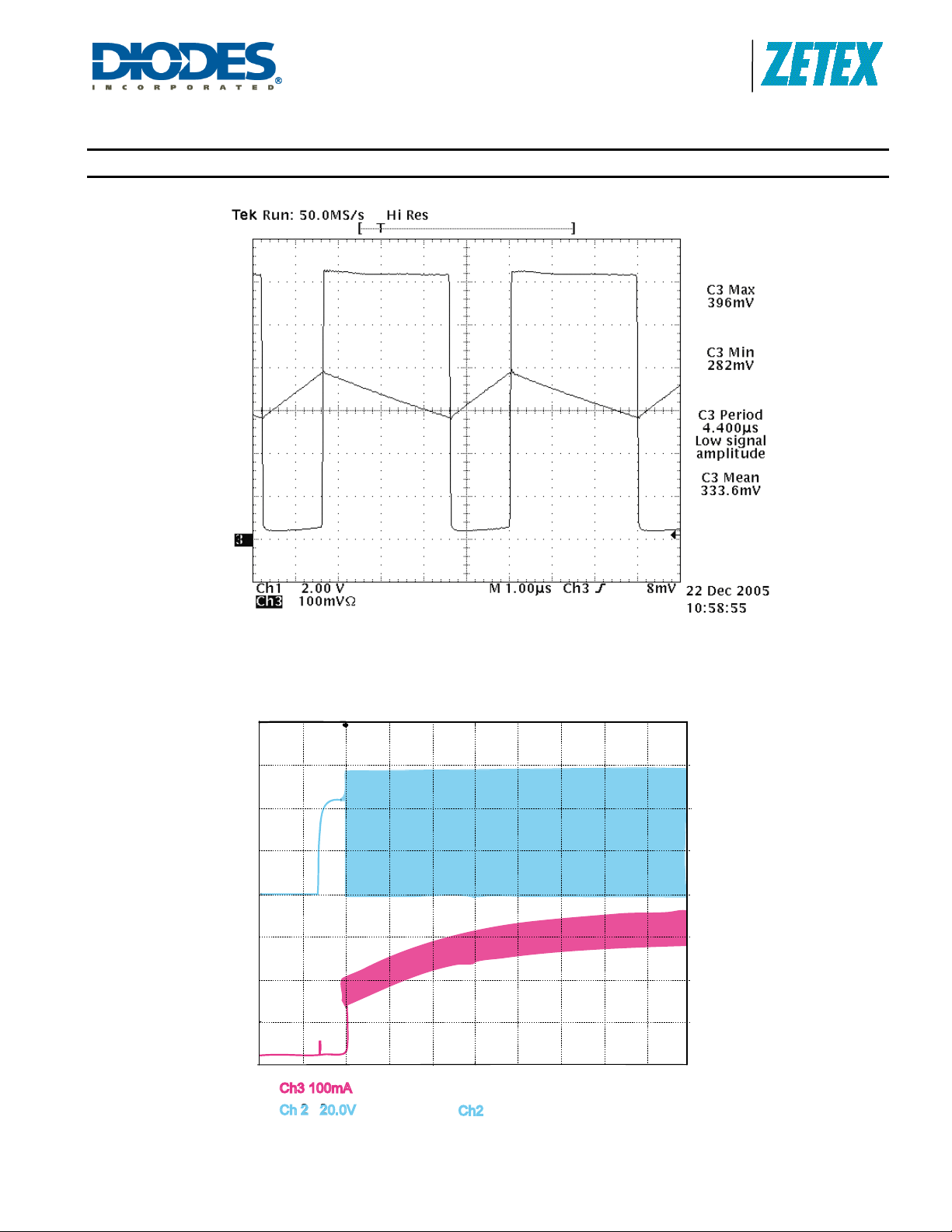
Typical Operating Waveforms [V
Normal Operation. Output Current (Ch3) and LX Voltage (Ch1)
ZXLD1352
Document number: DS33469 Rev. 3 - 2
2
3
Ch3 100mA
Ch 2 20.0V
Start-up Waveforms. Output Current (Ch3), LX Voltage (Ch2)
= 12V, R
IN
= 0.3Ω, L = 100µH]
S
M 400μs5.0S/s
\ 12.0 V
ACh2
7 of 21
www.diodes.com
200 ns/pt
December 2010
© Diodes Incorporated
 Loading...