

Page 1
A
Product Line o
f
Diodes Incorporated
ZXLD1350
30V 350mA LED DRIVER with AEC-Q100
Description
The ZXLD1350 is a hysteretic mode inductive step-down
converter with integrated switch and high side current sense.
It operates from an input supply from 7V to 30V driving single
or multiple series connected LEDs efficiently external
adjustable output current up to 350mA.
The ZXLD1350 has been qualified to AECQ100 grade 2
allowing it to operate at ambient temperatures from -40 to
105°C.
The output current can be adjusted by applyi ng a DC voltage
or a PWM waveform. 100:1 adjustment of output current is
possible using PWM control. Applying a voltage of 0.2V or
lower to the ADJ pin turns the output off and switches the
device into a low current standby state.
Features
• Simple low parts count
• Internal 30V NDMOS switch
• Internal PWM filter
• High efficiency (up to 95% (Note 1)
• Wide input voltage range: 7V to 30V
• 40V transient capability
• Up to 1MHz switching frequency
• Typical 4% output current accuracy
• Qualified to AEC-Q100 Grade 2
• Available in “Green” Molding Compound (No Br, Sb)
• Lead Free Finish/ RoHS Compliant (Note 2)
Notes: 1. Using standard external components as specified under electrical characteristics. Efficiency is dependent upon the number of LEDs driven and on
2. EU Directive 2002/95/EC (RoHS). All applicable RoHS exemptions applied. Please visit our website at:
external component types and values.
http://www.diodes.com/products/lead_free.html
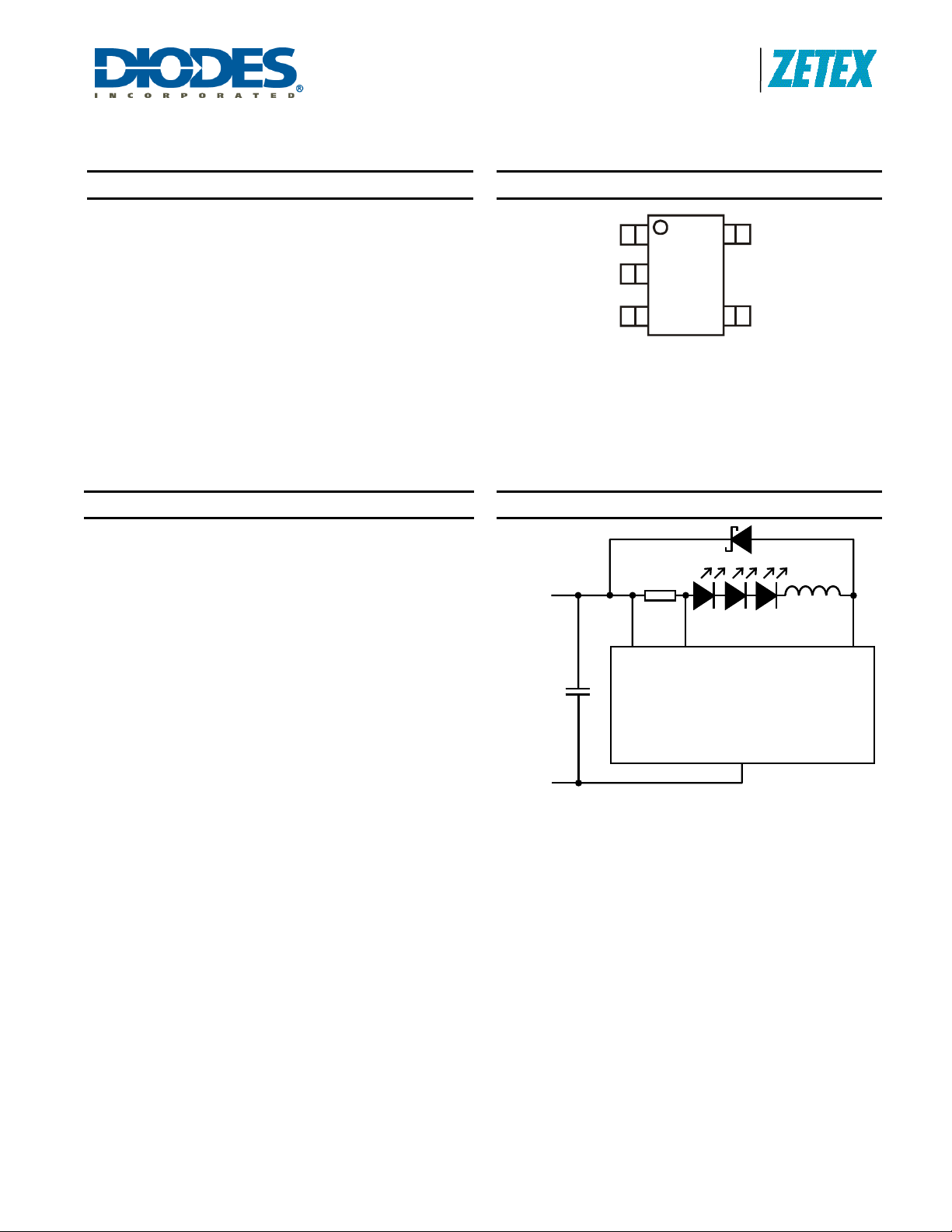
Pin Assignments
LX
GND
ADJ
TSOT23-5
To p View
Typical Application Circuit
R
0.33Ω
V
IN
S
SET
ZXLD1350
GND
V
IN
7~30V
C1
1µF
GND
ADJ
V
IN
I
SENSE
L1
47µH
LX
ZXLD1350
Document number: DS33468 Rev. 8 - 2
1 of 22
www.diodes.com
March 2011
© Diodes Incorporated
Page 2
A
f
V
Block Diagram
Product Line o
Diodes Incorporated
ZXLD1350
30V 350mA LED DRIVER with AEC-Q100
R
IN
V
IN
Voltage
regulator
C1
ADJ
200k
Vref
1.25V
GND
4KHz
5V
Shutdown
circuit
V
IN
R1
R2
R3
Current sense circuit
Figure 1. Block diagram – Pin Connection
S
D1
-
+
Comparator
-
+
I
SENSE
L1
LX
MN
Pin Description
Name Pin No. Description
LX 1 Drain of NDMOS switch
GND 2 Ground (0V)
Multi-function On/Off and brightness control pin:
• Leave floating for normal operation.(V
I
OUTnom
=0.1/RS)
• Drive to voltage below 0.2V to turn off output current
ADJ 3
• Drive with DC voltage (0.3V<V
ADJ
• Drive with PWM signal from open-collector or open-drain transistor, to adjust output current.
Adjustment range 25% to 100% of I
• Connect a capacitor from this pin to ground to increase soft-start time. (Default soft-start time=0.5ms.
Additional soft-start time is approx.0.5ms/nF)
I
SENSE
VIN
4
5
Connect resistor R
(Note: R
SMIN
Input voltage (7V to 30V). Decouple to ground with 1µF of higher X7R ceramic capacitor close to
device
ZXLD1350
Document number: DS33468 Rev. 8 - 2
from this to VIN to define nominal average output current I
S
=0.27V with ADJ pin open circuit)
www.diodes.com
= V
ADJ
=1.25V giving nominal average output current
REF
<2.5V) to adjust output current from 25% to 200%
OUTnom
2 of 22
for f>10kHz and 1% to 100% of I
OUTnom
OUTnom
(†)
of I
OUTnom
for f<500Hz
=0.1/RS
March 2011
© Diodes Incorporated
Page 3
A
Product Line o
f
Diodes Incorporated
ZXLD1350
30V 350mA LED DRIVER with AEC-Q100
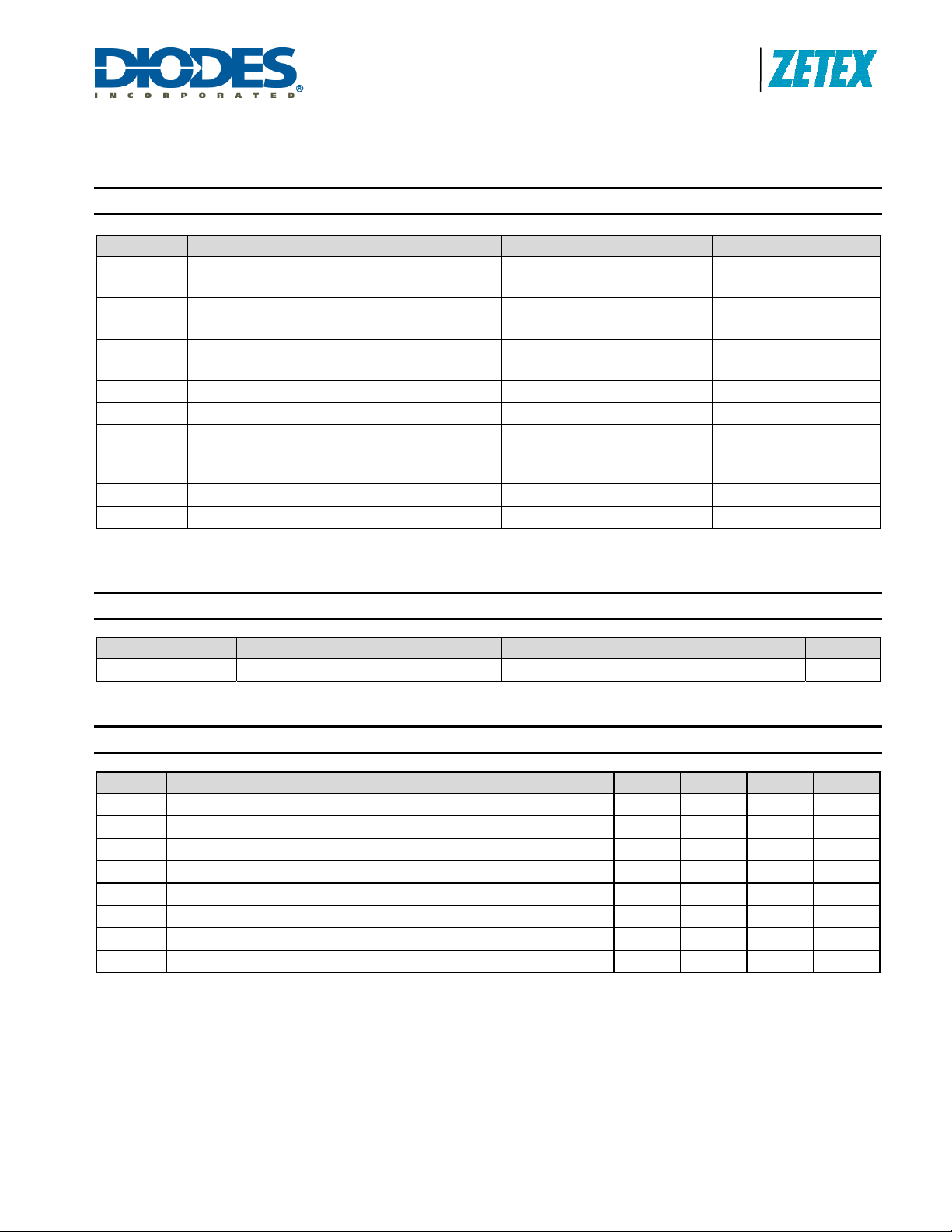
Absolute Maximum Ratings (Voltages to GND Unless Otherwise Stated)
Symbol Parameter Rating Unit
VIN
V
SENSE
VLX
V
ILX
ADJ
Input Voltage
I
SENSE
Voltage
(measured with respect to VIN)
LX Output Voltage
Adjust Pin Input Voltage -0.3 to +6 V
Switch Output Current 500 mA
Power Dissipation
P
TOT
(Refer to Package thermal de-rating curve on
page 19)
TST
TJ
MAX
These are stress ratings only. Operation above the absolute maximum rating may cause device failure. Operation at the absolute maximum ratings, for extended
periods, may reduce device reliability.
Storage Temperature -55 to 150 °C
Junction Temperature 150 °C
-0.3 to +30
(40V for 0.5 sec)
+0.3 to -5
-0.3 to +30
(40V for 0.5 sec)
V
V
V
450 mW
Thermal Resistance
Symbol Parameter Rating Unit
θ
JA
Junction to Ambient 200 °C/W
Recommended Operating Conditions
Symbol Parameter Min Typ. Max Units
VIN
t
OFFMIN
t
ONMIN
DLX
I
LX_CONT
f
LXmax
TPD
ZXLD1350
Document number: DS33468 Rev. 8 - 2
Input voltage 7
Minimum switch off-time
Minimum switch on-time
Duty cycle range 0.01
TA
Ambient operating temperature range -40
Average/RMS LX switch current 0.37 A
Recommended maximum operating frequency 1 MHz
Internal comparator propagation delay 50 ns
3 of 22
www.diodes.com
30 V
800 ns
800 ns
0.99
+105 °C
March 2011
© Diodes Incorporated
Page 4
A
Product Line o
f
Diodes Incorporated
ZXLD1350
30V 350mA LED DRIVER with AEC-Q100
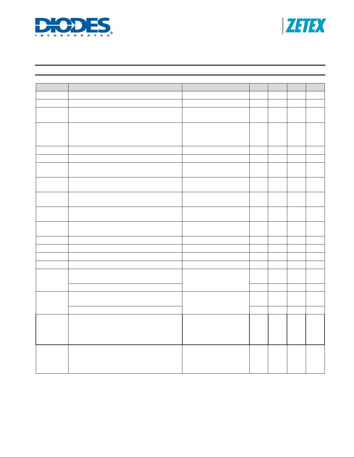
Electrical Characteristics (Test conditions: V
= 12V, T
IN
= 25°C, unless otherwise specified.) (Note 3)
amb
Symbol Parameter Condition Min. Typ. Max. Unit
VSU
I
INQoff
I
INQon
V
SENSE
V
SENSEHYS
I
SENSE
V
REF
DV
REF
V
ADJ
V
ADJoff
V
ADJon
R
Resistance between ADJ pin and V
ADJ
I
LXmean
RLX
I
LX(leak)
Internal regulator start-up threshold
Quiescent supply current with output off ADJ pin grounded 15 20 µA
Quiescent supply current with output switching
Mean current sense threshold voltage
(Defines LED current setting accuracy)
Sense threshold hysteresis ±15 %
I
pin input current V
SENSE
Internal reference voltage
/DT Temperature coefficient of V
External control voltage range on ADJ pin for
DC brightness control (Note 4)
DC voltage on ADJ pin to switch device from
active (on) state to quiescent (off) state
DC voltage on ADJ pin to switch device from
quiescent (off) state to active (on) state
Continuous LX switch current 0.37 A
LX switch ‘On’ resistance 1.5 2
LX switch leakage current 1 µA
Duty cycle range of PWM signal applied to ADJ
D
PWM(LF)
pin during low frequency PWM dimming mode
Brightness control range 100:1
Duty cycle range of PWM signal applied to ADJ
D
PWM(HF)
pin during high frequency PWM dimming mode
Brightness control range 5:1
fLX
Operating frequency
(See graphs for more details)
REF
REF
VIN rising
ADJ pin floating
f = 250kHz
Measured on I
with respect to V
V
= 1.25V
ADJ
= V
SENSE
IN
SENSE
IN
-0.1
pin
Measured on ADJ pin with
pin floating
50
4.8 V
250 500 µA
95 100 105 mV
1.25 10 µA
1.21 1.25 1.29 V
ppm/°
C
0.3 2.5 V
V
V
ADJ
ADJ
falling
rising
0.15 0.2 0.25 V
0.2 0.25 0.3 V
135 250 k
PWM frequency <500Hz
PWM amplitude = V
REF
0.01 1
Measured on ADJ pin
PWM frequency <10kHz
PWM amplitude = V
REF
0.16 1
Measured on ADJ pin
ADJ pin floating
L = 100H (0.82V)
= 350ma @ V
I
OUT
Driving 1 LED
LED
= 3.4V
250 kHz
Time taken for output
tSS
Start up time
(See graphs for more details)
current to reach 90% of final
value after voltage on ADJ
500 µs
pin has risen above 0.3V.
Notes: 3. Production testing of the device is performed at 25°C. Functional operation of the device and parameters specified over a -40°C to +105°C
temperature range, are guaranteed by design, characterization and process control.
4. 100% brightness corresponds to V
proportionally.
ZXLD1350
Document number: DS33468 Rev. 8 - 2
ADJ
= V
ADJ(nom)
= V
. Driving the ADJ pin above V
REF
4 of 22
www.diodes.com
will increase the V
REF
threshold and output current
SENSE
© Diodes Incorporated
March 2011
Page 5

A
Product Line o
f
Diodes Incorporated
ZXLD1350
30V 350mA LED DRIVER with AEC-Q100
Device Description
The device, in conjunction with the coil (L1) and current sense resistor (RS), forms a self-oscillating continuous-mode buck
converter.
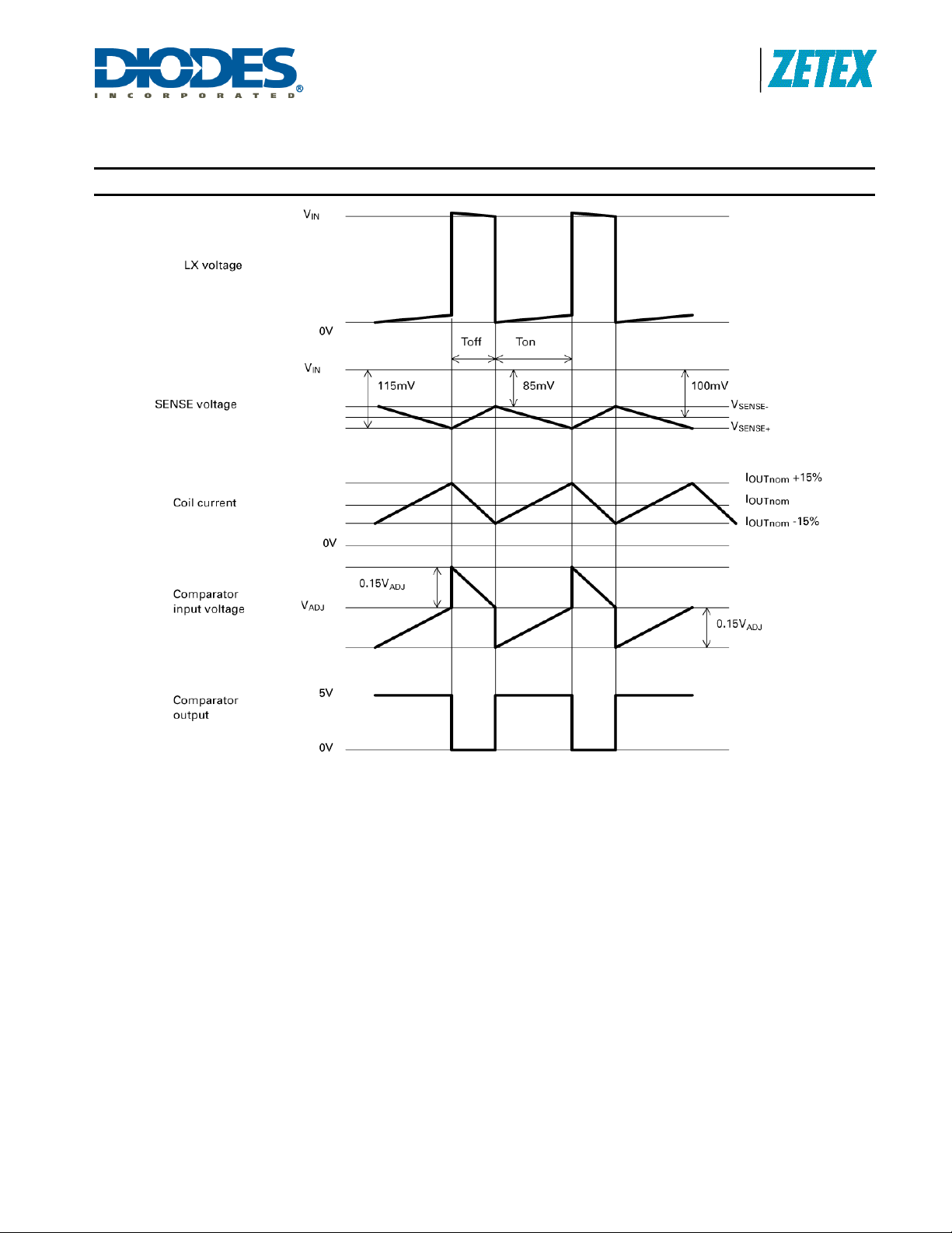
Device operation (Refer to block diagram and Figure 1 - Operating waveforms)
Operation can be best understood by assuming that the ADJ pin of the device is unconnected a nd the voltage on this pin
) appears directly at the (+) input of the comparator.
(V
ADJ
When input voltage V
circuit. Under this condition, the (-) input to the comparator is at ground and its output is high. This turns MN on and switches
the LX pin low, causing current to flow from V
by V
and L1 to produce a voltage ramp (V
IN
resistor R1 by the current sense circuit and produces a proportional current in internal resistors R2 and R3. T his produces a
ground referred rising voltage at the (-) input of the comparator. When this reaches the threshold voltage (V
comparator output switches low and MN turns off. The comparator output also drives another NMOS switch, which bypasses
internal resistor R3 to provide a controlled amount of hysteresis. The hysteresis is set by R3 to be nominally 15% of V
When MN is off, the current in L1 continues to flow via D1 and the LED(s) back to V
determined by the LED and diode forward voltages to produce a falling voltage at the input of the comparator. When this
voltage returns to V
ramping between limits of V
Switching thresholds
With V
I
SENSE
I
OUTnom
Nominal ripple current is ±15mV/R
=V
ADJ
REF
pin with respect to VIN). The average output current I
=100mV/RS
Adjusting output current
The device contains a low pass filter between the ADJ pin and the threshold comparator and an internal current limiting
resistor (200k nom) between ADJ and the internal reference voltage. This allows the ADJ pin to be overdriven with either
DC or pulse signals to change the V
comprising three sections, each with a cut-off frequency of nominally 4kHz.
Details of the different modes of adjusting output current are given in the applications section.
Output shutdown
The output of the low pass filter drives the shutdown circuit. When the input voltage to this circuit falls below the threshold
(0.2V nom), the internal regulator and the output switch are turned off. The voltage reference remains powered during
shutdown to provide the bias current for the shutdown circuit. Quiescent supply current during shutdown is nominally
15mA and switch leakage is below 1mA.
ZXLD1350
Document number: DS33468 Rev. 8 - 2
is first applied, the initial current in L1 and RS is zero and there is no output from the current sense
IN
to ground, via RS, L1 and the LED(s). The current rises at a rate determined
IN
) across RS. The supply referred voltage V
SENSE
IN
, the comparator output switches high again. This cycle of events repeats, with the comparator inpu t
ADJ
± 15%.
ADJ
, the ratios of R1, R2 and R3, define an average V
is then defined by this voltage and Rs according to:
OUTnom
S
switching threshold and adjust the output current. The filter is third order,
SENSE
5 of 22
www.diodes.com
switching threshold of 100mV (measured on the
SENSE
is forced across internal
SENSE
. The current decays at a rate
© Diodes Incorporated
), the
ADJ
.
ADJ
March 2011
Page 6
A
f
Device Description (Continued)
Figure 1. Theoretical Operating Waveforms
Product Line o
Diodes Incorporated
ZXLD1350
30V 350mA LED DRIVER with AEC-Q100
ZXLD1350
Document number: DS33468 Rev. 8 - 2
6 of 22
www.diodes.com
March 2011
© Diodes Incorporated
Page 7
A
Product Line o
f
Diodes Incorporated
ZXLD1350
30V 350mA LED DRIVER with AEC-Q100
Device Description (Continued)
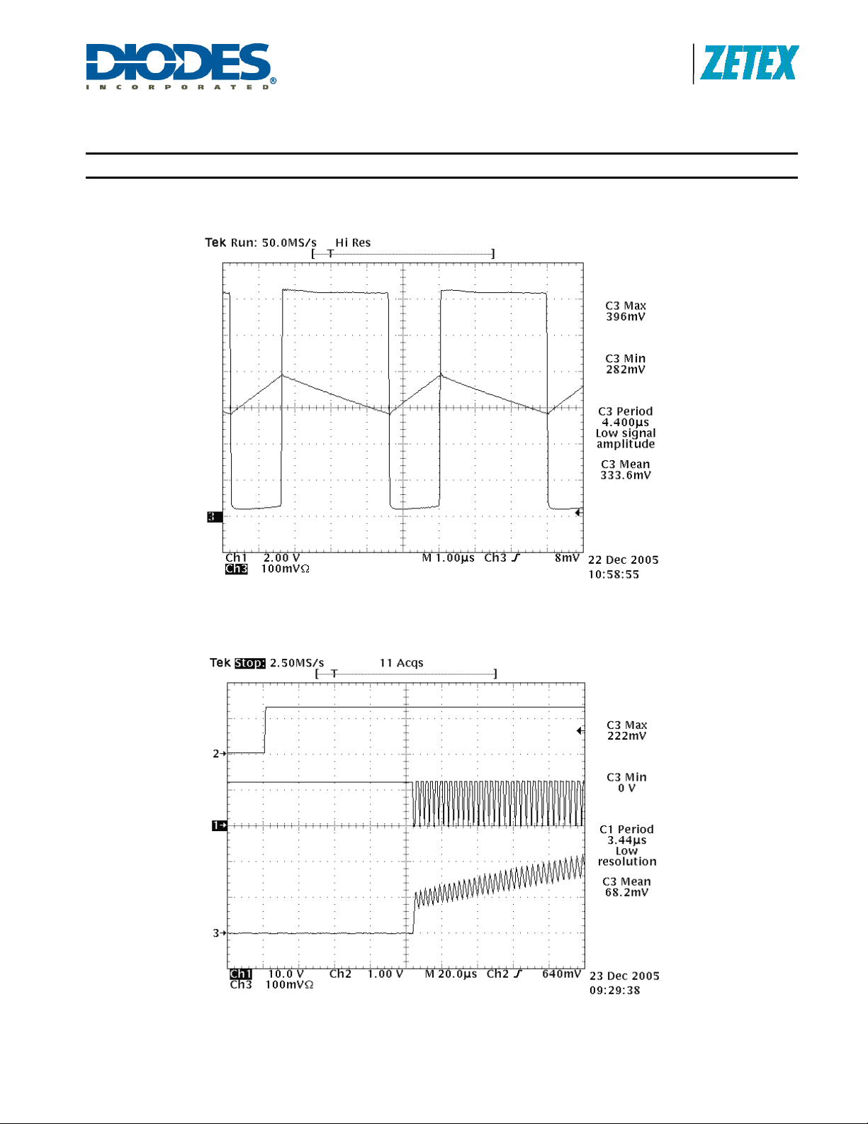
Typical Operating Waveforms [VIN = 12V, RS = 0.3V, L = 100 μH]
Normal operation. Output current (Ch3) and LX voltage (Ch1)
Start-up waveforms. Output current (Ch3), LX voltage (Ch1) and V
ZXLD1350
Document number: DS33468 Rev. 8 - 2
7 of 22
www.diodes.com
ADJ
(Ch2)
March 2011
© Diodes Incorporated
Page 8

A
f
Typical Operating Conditions
Product Line o
Diodes Incorporated
ZXLD1350
30V 350mA LED DRIVER with AEC-Q100
ZXLD1350
Document number: DS33468 Rev. 8 - 2
8 of 22
www.diodes.com
March 2011
© Diodes Incorporated
Page 9

A
f
Typical Characteristics (Continued)
Product Line o
Diodes Incorporated
ZXLD1350
30V 350mA LED DRIVER with AEC-Q100
ZXLD1350
Document number: DS33468 Rev. 8 - 2
9 of 22
www.diodes.com
March 2011
© Diodes Incorporated
Page 10

A
f
Typical Characteristics (Continued)
Product Line o
Diodes Incorporated
ZXLD1350
30V 350mA LED DRIVER with AEC-Q100
ZXLD1350
Document number: DS33468 Rev. 8 - 2
10 of 22
www.diodes.com
March 2011
© Diodes Incorporated
Page 11

A
f
Typical Characteristics (Continued)
Product Line o
Diodes Incorporated
ZXLD1350
30V 350mA LED DRIVER with AEC-Q100
ZXLD1350
Document number: DS33468 Rev. 8 - 2
11 of 22
www.diodes.com
March 2011
© Diodes Incorporated
Page 12

A
Product Line o
f
Diodes Incorporated
ZXLD1350
30V 350mA LED DRIVER with AEC-Q100
Application Information
Setting nominal average output current with external resistor R
The nominal average output current in the LED(s) is determined by the value of the external current sense resistor (RS)
connected between V
and I
IN
and is given by:
SENSE
S
I
= 0.1/RS [for RS > 0.27]
OUTnom
The table below gives values of nominal average o utput current for several pr eferred values of current setting res istor (RS) in
the typical application circuit shown on page 1:
RS(Ω)
Nominal average output
current (mA)
0.27 370
0.30 333
0.33 300
0.39 256
The above values assume that the ADJ pin is floating and at a nomina l voltage of V
(=1.25V). Note that RS = 0.27V is the
REF
minimum allowed value of sense resistor under these conditions to maintain s witch current below the specified maximum
value.
It is possible to use different values of RS if the ADJ pin is driven from an external voltage. (See next section).
Output current adjustment by external DC control voltage
The ADJ pin can be driven by an external dc voltage (V
GND
.
S
the nominal average value defined by R
+
DC
GND
ADJ
ZXLD1350
The nominal average output current in this case is given by:
), as shown, to adjust the output current to a value above or below
ADJ
I
= 0.08*V
OUTdc
Note that 100% brightness setting corresponds to V
increased in proportion to prevent I
/RS for 0.3 < V
ADJ
< 2.5V
ADJ
ADJ
exceeding 370mA maximum.
OUTdc
= V
. When driving the ADJ pin above 1.25V, RS must be
REF
The input impedance of the ADJ pin is 200k ±25%.
ZXLD1350
Document number: DS33468 Rev. 8 - 2
12 of 22
www.diodes.com
March 2011
© Diodes Incorporated
Page 13

A
Product Line o
f
Diodes Incorporated
ZXLD1350
30V 350mA LED DRIVER with AEC-Q100
Application Information (Continued)
Output Current Adjustment by PWM Control
Directly driving ADJ input
A Pulse Width Modulated (PWM) signal with duty cycle D
output current to a value above or below the nominal average value set by resistor R
GND
PWM
ADJ
ZXLD1350
GND
V
ADJ
0V
Driving the ADJ input via open collector transistor
The recommended method of driving the ADJ pin and contr olling the amplit ude of the PWM waveform is to use a small NPN
switching transistor as shown below:
can be applied to the ADJ pin, as shown below, to adjust the
PWM
:
S
PWM
This scheme uses the 200k resistor between the ADJ pin and the internal v oltage reference as a pull-up resistor for the
external transistor.
GND
ADJ ZXLD1350
GND
Driving the ADJ input from a microcontroller
Another possibility is to drive the device from the open drain output of a microcontroller. The diagram below shows one
method of doing this:
MCU
The diode and resistor suppress possible high amplitude negative spikes on the ADJ input resulting fr om the drain-source
capacitance of the FET. Negative spikes at the input to the device should be avoid ed as they may cause errors in output
current, or erratic device operation.
PWM dimming can be further split into high frequency and low frequency PWM dimming and how the device responds to
these.
ZXLD1350
Document number: DS33468 Rev. 8 - 2
10k
ADJ
ZXLD1350
GND
13 of 22
www.diodes.com
March 2011
© Diodes Incorporated
Page 14

A
Product Line o
f
Diodes Incorporated
ZXLD1350
30V 350mA LED DRIVER with AEC-Q100
Application Information (Continued)
Low frequency PWM mode
When the ADJ pin is driven with a low frequency PWM si gnal (eg 100Hz), with a high level voltage V
zero, the output of the internal low pass filter will s wing between 0V and V
below its turn-off threshold (200mV nom) when the ADJ pin is low. This will cause the output curre nt to be switched on and off
at the PWM frequency, resulting in an average output current I
frequency PWM operating waveforms).
Figure 2. Low frequency PWM operating waveforms
The average value of output current in this mode is given by:
I
0.1D
OUTavg
This mode is preferable if optimum LED 'whiteness' is required. It will also provide the widest possible dimming range
(approx. 100:1) and higher efficiency at the expense of greater output ripple.
Note that the low pass filter introduces a small error in the o utput duty cycle due to the difference bet ween the start-up and
shut-down times. This time difference is a result of the 200mV s hutdown threshold an d the rise and fall times at th e output of
the filter. To minimize this error, the PWM duty cycle should be as low as possible consistent with avoiding flicker in the LED.
PWM/RS
for D
PWM
>0 01
proportional to the PWM duty cycle. (See Figure 2 - Low
OUTavg
, causing the input to the shutdown circuit to fall
ADJ
and a low level of
ADJ
ZXLD1350
Document number: DS33468 Rev. 8 - 2
14 of 22
www.diodes.com
March 2011
© Diodes Incorporated
Page 15

A
Product Line o
f
Diodes Incorporated
ZXLD1350
30V 350mA LED DRIVER with AEC-Q100
Application Information (Continued)
High frequency PWM mode
At PWM frequencies above 10kHz and for duty cycles a bove 0.16, the output of the internal low pass filter will contain a
DC component that is always above the shutdown threshold. This will maintain continuous device operation and the n ominal
average output current will be proportional to the average v oltage at the output of the filter, which is directly proportional to the
duty cycle. (See Figure 3 – High frequency PW M operating waveforms). For best results, the PWM frequency should be
maintained above the minimum specified value of 10kHz, in order to minimize ripple at the output of the filter. The shutdo wn
comparator has approximately 50mV of hysteresis, to minimize erratic s witching due to this ripple. An upper PWM frequenc y
limit of approximately one tenth of the oper ating frequency is recommended, to avoid excessive output modulation and to
avoid injecting excessive noise into the internal reference.
Figure 3. High Frequency PWM operating waveforms
The nominal average value of output current in this mode is given by:
I
»0.1D
OUTnom
This mode will give minimum output ripple and r educed radiated emission, but with a reduced dimming rang e (approx.5:1).
The restricted dimming range is a result of the device being turne d off when the DC c omponent on the f ilter output fal ls bel o w
200mV.
PWM/RS
Shutdown mode
Taking the ADJ pin to a voltage below 0.2V for more than appr oximately 100 s, will turn off the output and s upply current will
fall to a low standby level of 15A nominal.
Note that the ADJ pin is not a logic input. Taking the ADJ pin to a voltage abov e V
100% nominal average value. (See graphs for details).
for D
PWM
>0.16
will increase output current above the
REF
ZXLD1350
Document number: DS33468 Rev. 8 - 2
15 of 22
www.diodes.com
March 2011
© Diodes Incorporated
Page 16

A
Product Line o
f
Diodes Incorporated
ZXLD1350
30V 350mA LED DRIVER with AEC-Q100
Application Information (Continued)
Soft-start
The device has inbuilt soft-start action due to the delay through the PW M filter. An external capacitor from the ADJ pin to
ground will provide additional soft-start delay, by increasin g the time taken for the voltage on this pin to rise to the turn-on
threshold and by slowing down the rate of rise of the control voltage at the input of the comparator. With no external
capacitor, the time taken for the output to reach 90% of its final value is approximately 500 s. Adding capacitance i ncreases
this delay by approximately 0.5ms/nF.
The graph below shows the variation of soft-start time for different values of capacitor.
Inherent open-circuit LED protection
If the connection to the LED(s) is open-circuited, the coil is isolated from the LX pin of the chip, so the device will not be
damaged, unlike in many boost converters, where the bac k EMF may damage the inter nal switch by forcing the drai n above
its breakdown voltage.
Capacitor selection
A low ESR capacitor should be used for input decoupl ing, as the ESR of this capacitor appears in series with the supply
source impedance and lowers overall efficiency. This capacitor has to supply the relatively high peak current to the coil and
smooth the current ripple on the input supply. A minimum value of 1F is acceptable if the in put sourc e is close to the devic e,
but higher values will improve performance at lower input voltages, especi ally when the source impedan ce is high. The input
capacitor should be placed as close as possible to the IC.
For maximum stability over temperature and voltage, capacitors with X7R, X5R, or better dielectric are recommended.
Capacitors with Y5V dielectric are not suitable for decoupling in this application and should NOT be used.
A table of recommended manufacturers is provided below:
Manufacturer Website
Murata www.murata.com
Taiyo Yuden www.t-yuden.com
Kemet www.kemet.com
AVX www.avxcorp.com
ZXLD1350
Document number: DS33468 Rev. 8 - 2
16 of 22
www.diodes.com
March 2011
© Diodes Incorporated
Page 17

A
Product Line o
f
Diodes Incorporated
ZXLD1350
30V 350mA LED DRIVER with AEC-Q100
Application Information (Continued)
Inductor Selection
Recommended inductor values for the ZXLD1350 are in the range 47µH to 220µH.
Higher values of inductance are recommended at higher supply volt ages in order to minimize errors due to s witching delays,
which result in increased ripple and lower efficiency. Higher va lues of inductance also result in a smaller change in output
current over the supply voltage range. (See grap hs). The inductor shou ld be mounted as close to the device as possible with
low resistance connections to the LX and V
The chosen coil should have a saturation current higher than the peak output current and a continuous
current rating above the required mean output current.
Suitable coils for use with the ZXLD1350 are listed in the table below:
pins.
IN
Part No.
L
(µH)
DO1608C 47 0.64 0.5
47 0.38 0.56
MSS6132ML
68 0.58 0.47
100 0.82 0.39
CD104-MC 220 0.55 0.53 Sumida
NP04SB470M 47 0.27 0.38 Taiyo Yuden
DCR
(V)
I
SAT
(A)
Manufacturer
CoilCraft
The inductor value should be chosen to maintain o per ating dut y c ycle a nd switch 'on' /'off' times within the specified limits over
the supply voltage and load current range.
The following equations can be used as a guide, with reference to Figure 1 - Operating waveforms.
LX Switch 'On' time
IL
t
=
ON
t
ONnmin
> 200ns
Note:
LX Switch 'Off' time
=
t
OFF
t
OFFmin
> 200ns
Note:
Where:
L is the coil inductance (H)
r
is the coil resistance (Ω)
L
I
is the required LED current (A)
avg
ΔI is the coil peak-peak ripple current (A) {Internally set to 0.3 x I
is the supply voltage (V)
V
IN
V
is the total LED forward voltage (V)
LED
is the switch resistance (Ω)
R
LX
is the rectifier diode forward voltage at the required load current (V)
V
D
Δ
()
Δ
IL
+×++
()
rRIVV
LSavgDLED
RrRIVV
++×−−
LXLSavgLEDIN
avg
}
ZXLD1350
Document number: DS33468 Rev. 8 - 2
17 of 22
www.diodes.com
March 2011
© Diodes Incorporated
Page 18

A
Product Line o
f
Diodes Incorporated
ZXLD1350
30V 350mA LED DRIVER with AEC-Q100
Application Information (Continued)
Example:
For VIN =12V, L=47µH, rL=0.64V, V
t
= (47e-6 x 0.105)/(12 - 3.4 - 0.672) = 0.622µs
ON
t
= (47e-6 x 0.105)/(3.4 + 0.36 + 0.322)= 1.21µs
OFF
This gives an operating frequency of 546kHz and a duty cycle of 0.34.
These and other equations are available as a spreadsh eet calculator from the Diodes website.
Note that in practice, the duty c ycle and ope rating fr equency will deviat e from the c alculated v alues due to dynamic s witchin g
delays, switch rise/fall times and losses in the external compon ents.
Optimum performance will be achieved by setting the duty cycle close to 0.5 at the nominal supply voltage. This helps to
equalize the undershoot and overshoot and improves temperature stability of the output current.
LED
=3.4V, I
=350mA and VD =0.36V
avg
Diode Selection
For maximum efficiency and performance, the rectifier (D1 ) should be a fast lo w capacitance Schottk y diode with low reverse
leakage at the maximum operating voltage and tem perature. The recommende d diode for use with this part is the Z LLS1000.
This has approximately ten times lower leakage than stand ard Schottky diodes, which are unsuitable fo r use above 85°C. It
also provides better efficiency than silicon dio des, due to a combination of lower forward voltage an d reduced recovery time.
The table below gives the typical characteristics for the ZLLS1000:
Diode
Forward Voltage
@ 100mA (mV)
Continuous
Current
(mA)
Reverse Leakage
@ 30V 85°C
(mA)
Package
ZLLS1000 310 1000 300 TSOT23
If alternative diodes are used, it is important to select parts with a peak current rating above the peak coil current and a
continuous current rating higher than th e maxim um output load current. It i s very import ant t o consider t he r everse lea kage o f
the diode when operating above 85°C. Excess leakage will increase the power dissipation in the device.
The higher forward voltage and overshoot due to reverse recovery time in silicon diodes will incre ase the peak voltage on the
LX output. If a silicon diode is used, care should be taken to ensure that the total voltage appearing on the LX pin including
supply ripple, does not exceed the specified maximum val ue.
Reducing Output Ripple
Peak to peak ripple current in the LED(s) can be reduced, if required, by shunting a capacitor Cled across the LED(s ) as
shown below:
V
IN
R
S
LED
L1
D1
V
IN
I
SENSE
LX
Cled
ZXLD1350
ZXLD1350
Document number: DS33468 Rev. 8 - 2
18 of 22
www.diodes.com
March 2011
© Diodes Incorporated
Page 19

A
Product Line o
f
Diodes Incorporated
ZXLD1350
30V 350mA LED DRIVER with AEC-Q100
Application Information (Continued)
A value of 1F will reduce nominal ripple current by a factor three (appro x.). Proportionally lo wer ripple can be achieved with
higher capacitor values. Note that the capacitor will not affect operating frequency or efficiency, but it will increase start-up
delay, by reducing the rate of rise of LED voltage.
Operation at low supply voltage
The internal regulator disables the driv e to the switch until the supply has risen above the start-up t hreshold (VSU). Above
this threshold, the device will start to operate. However, with the supply voltage below the specified minimum value, the
switch duty cycle will be high and the device po wer dissipat i on will be at a maximum. Car e should be t ak en t o avoi d o p eratin g
the device under such conditions in the application, in order to minimize the risk of exceeding the maximum allowed die
temperature. (See next section on thermal considerati ons).
Note that when driving loads of two or more LEDs, the forward drop will normally be sufficient to prevent the device from
switching below approximately 6V. This will minimize the risk of damage to the device.
Thermal considerations
When operating the device at high ambient temperatures, or when driving maximum load current, care must be taken to avoid
exceeding the package power dissipation limits. The graph below gives details for power derating. This assum es the device
to be mounted on a (25mm)
Note that the device power dissipation will most often be a maximum at minimum supply volt age. It will also increase if the
efficiency of the circuit is low. This ma y result from the use of unsuitable coils, or excessive parasitic output capacit ance on
the switch output.
2
PCB with 1oz copper standing in still air.
Thermal compensation of output current
High luminance LEDs often need to be supplied with a temperature compensated cur rent in order to maintain stable and
reliable operation at all drive levels. The LEDs are usually mounted remotely from the device, so for this reason, the
temperature coefficients of the internal circuits for the ZXLD1350 have been optimized to minimize the change in output
current when no compensation is employed. If output current compensation is required, it is possible to use an external
temperature sensing network - normally using Negative T emperature Coefficient (NTC) thermistors and/or diodes, mounted
very close to the LED(s). The output of the sensing network can be used to drive the ADJ pin in order to reduce output current
with increasing temperature.
ZXLD1350
Document number: DS33468 Rev. 8 - 2
19 of 22
www.diodes.com
March 2011
© Diodes Incorporated
Page 20

A
Product Line o
f
Diodes Incorporated
ZXLD1350
30V 350mA LED DRIVER with AEC-Q100
Application Information (Continued)
Layout considerations
LX pin
The LX pin of the device is a fast s witching node, so PCB tracks should be kept as sh ort as possible. To minimize ground
'bounce', the ground pin of the device should be soldered directly to the ground plane.
Coil and decoupling capacitors
It is particularly important to mount the coil and the input decoupling capacitor close to the device to minimize parasitic
resistance and inductance, which will degra de efficiency. It is als o important to take acc ount of any tra ck resistance in serie s
with current sense resistor RS.
ADJ pin
The ADJ pin is a high impedance input, so when left f loating, PCB tracks to this pin sho uld be as short as possible to r educe
noise pickup. A 100nF capacitor from the ADJ pin to ground will reduce frequency modulation of the output under these
conditions. An additional series 10k resistor can also be used when driving the ADJ pin f rom an e xternal circu it (see be lo w).
This resistor will provide filtering for low frequenc y noise and provide protection against hi gh voltage transients.
10k
100nF
GND
ADJ
ZXLD1350
GND
High voltage tracks
Avoid running any high voltage tracks close to the ADJ pin, to re duce the risk of leakage due to board contamination. An y
such leakage may raise the ADJ pin volt age and cause excessive output current. A gr ound ring placed around the ADJ pin
will minimize changes in output current under these conditions.
ZXLD1350
Document number: DS33468 Rev. 8 - 2
20 of 22
www.diodes.com
March 2011
© Diodes Incorporated
Page 21

A
Product Line o
f
r
A
θ
Diodes Incorporated
ZXLD1350
30V 350mA LED DRIVER with AEC-Q100
Ordering Information
Device
ZXLD1350ET5TA 1350 ET5 TSOT23-5 180 8 3000 TA Grade 2
Note: 5. Pad layout as shown on Diodes Inc. suggested pad layout document AP02001, which can be found on our website at
http://www.diodes.com/datasheets/ap02001.pdf.
Part
Mark
Package
Code
Packaging
(Note 5)
Reel size
(mm)
Reel width
(mm)
Quantity
per reel
Part Numbe
Suffix
AEC-Q100
Level
Package Outline Dimensions
TSOT23-5
D
e1
E1
e
5x b
A2
A
A1
TSOT23-5
Dim Min Max Typ
E
L2
4x 1
θ
c
L
A
A1
A2
D
E
E1
b
c
e
e1
L
L2
θ
θ1
ll Dimensions in mm
1.00
−
0.01 0.10
0.84 0.90
− −
− −
− −
0.30 0.45
0.12 0.20
− −
− −
0.30 0.50
− −
0° 8° 4°
4° 12°
−
−
−
2.90
2.80
1.60
−
−
0.95
1.90
0.25
−
ZXLD1350
Document number: DS33468 Rev. 8 - 2
21 of 22
www.diodes.com
March 2011
© Diodes Incorporated
Page 22

A
Product Line o
f
Diodes Incorporated
ZXLD1350
30V 350mA LED DRIVER with AEC-Q100
DIODES INCORPORATED MAKES NO WARRANTY OF ANY KIND, EXPRESS OR IMPLIED, WITH REGARDS TO THIS DOCUMENT,
INCLUDING, BUT NOT LIMITED TO, THE IMPLIED WARRANTIES OF MERCHANTABILITY AND FITNESS FOR A PARTICULAR
PURPOSE (AND THEIR EQUIVALENTS UNDER THE LAWS OF ANY JURISDICTION).
Diodes Incorporated and its subsidiaries reserve the right to make modifications, enhancements, improvements, corrections or other changes
without further notice to this document and any product described herein. Diodes Incorporated does not assume any liability arising out of the
application or use of this document or any product described herein; neither does Diodes Incorporated convey any license under its patent or
trademark rights, nor the rights of others. Any Customer or user of this document or products des cribed herein in such applications shall
assume all risks of such use and will agree to hold Diodes Incorporated and all the companies whose products are represented on Diodes
Incorporated website, harmless against all damages.
Diodes Incorporated does not warrant or accept any liability whatsoever in respect of any products purchased through unauthorized sales
channel.
Should Customers purchase or use Diodes Incorporated products for any unintended or unauthorized application, Customers shall indemnify
and hold Diodes Incorporated and its representatives harmless against all claims, damages, expenses, and attorney fees arising out of,
directly or indirectly, any claim of personal injury or death associated with such unintended or unauthorized application.
Products described herein may be covered by one or more United States, international or foreign patents pending. Product names and
markings noted herein may also be covered by one or more United States, international or foreign trademarks.
Diodes Incorporated products are specifically not authorized for use as critical components in life support devices or systems without the
express written approval of the Chief Executive Officer of Diodes Incorporated. As used herein:
A. Life support devices or systems are devices or systems which:
1. are intended to implant into the body, or
2. support or sustain life and whose failure to perform when properly used in accordance with instructions for use provided in the
labeling can be reasonably expected to result in significant injury to the user.
B. A critical component is any component in a life support device or system whose failure to perform can be reasonably expected to cause
the failure of the life support device or to affect its safety or effectiveness.
Customers represent that they have all necessary expertise in the safety and regulatory ramifications of their life support devices or systems,
and acknowledge and agree that they are solely responsible for all legal, regulatory and safety-related requirements concerning their products
and any use of Diodes Incorporated products in such safety-critical, life support devices or systems, notwithstanding any devices- or systemsrelated information or support that may be provided by Diodes Incorporated. Further, Customers must fully indemnify Diodes Incorporated and
its representatives against any damages arising out of the use of Diodes Incorporated products in such safety-critical, life support devices or
systems.
Copyright © 2011, Diodes Incorporated
www.diodes.com
IMPORTANT NOTICE
LIFE SUPPORT
ZXLD1350
Document number: DS33468 Rev. 8 - 2
22 of 22
www.diodes.com
March 2011
© Diodes Incorporated
 Loading...