Diodes ZXLD1322 User Manual
A
Product Line o
f
Diodes Incorporated
ZXLD1322
BUCK/BOOST MODE DC-DC CONVERTER FOR LED DRIVING WITH 700mA OUTPUT AND CURRENT
CONTROL
Description
The ZXLD1322 is an inductive DC-DC converter, with an internal switch, designed for driving single or multiple LEDs in
series up to a total of 700mA output current. Applications cover input v oltages ranging from 2.5V to 15V. Depe nding upon
supply voltage and external components, this can provide up to 12W of output power. The device em ploys a variable 'on'
and 'off' time control scheme with adjustable peak switch current limiting and operates i n Buck/Boost mode, offering higher
power efficiency and lower system cost than conventional PFM buck/boost circuitry. The device includes the DC-DC
converter, a high-side current monitor and an NPN switching transistor to provide an integrated solution offering small PCB
size, competitive cost/performance, high power efficiency of DC-DC conversion and maximum L ED brightness/reliability.
More importantly, it retains design flexibility to add customer specific features. T he feedback control circuitry inside the
ZXLD1322 provides excellent load and current regul ation, resulting in very stable LED current over the useful life of the
battery and over the full operating temperature range. The LED curre nt can b e adjusted from 100 % down to 10% of t he set
value by applying a dc voltage to the ADJ pin and do wn to 1% b y appl ying a PWM sign al. An on-c hip LE D protecti on cir cuit
also allows output current to be reduced linearly above a predet erm ine d thresho ld temper ature using a n ext ernal thermi stor
at the TADJ pin. External resistors set nominal average LE D current a nd coil pe ak current indep endently. The dev ice can
be shut down by applying a continuous low level dc voltage to the ADJ pin.
Features
• 2.5V to 15V Input Voltage Range
• Up to 700mA output current
• Typical efficiency
• User-defined thermal control of LED
• output current using external thermistor
• High output current stability over input
• voltage and temperature
• 12A typical standby current
• LED current adjustable from 100%
• down to 2%
• Adjustable Soft-Start
• Capable of driving 3 LEDs in series
#
>80%
Applications
• High power LED flashlights
• LED back-up lighting
• General LED lighting
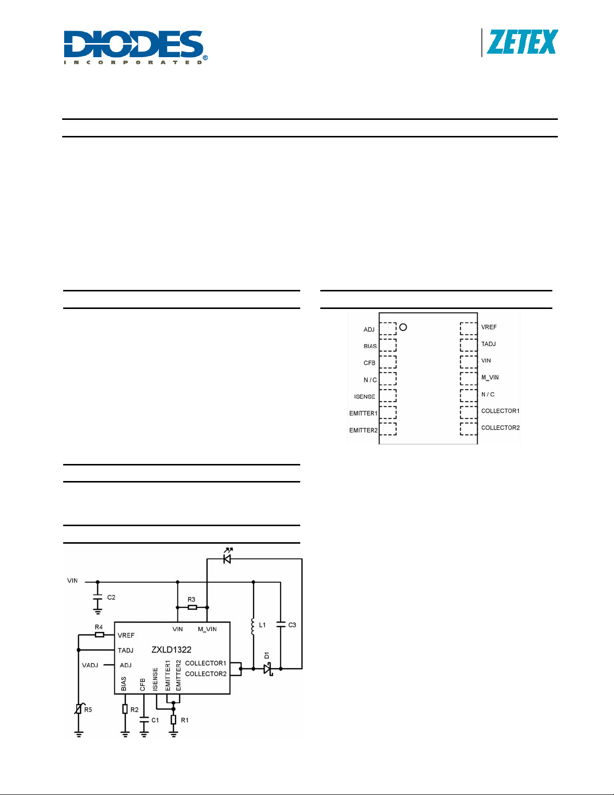
Typical Application Circuit
Pin Assignments
DFN4030-14 with Exposed Pad
0.50mm pitch
1.5W @ T
DFN4030-14 Package(Bottom View)
45° chamfer denote Pin 1
(Top View)
4mm x 3mm
= 70°C
A
Notes: #. Using standard external components as specified under electrical characteristics. Efficiency is dependent upon external component types and
values. Higher efficiency is possible with alternative coils.
ZXLD1322
Document number: DS32166 Rev. 3 - 2
1 of 17
www.diodes.com
April 2010
© Diodes Incorporated
A
Product Line o
f
Diodes Incorporated
ZXLD1322
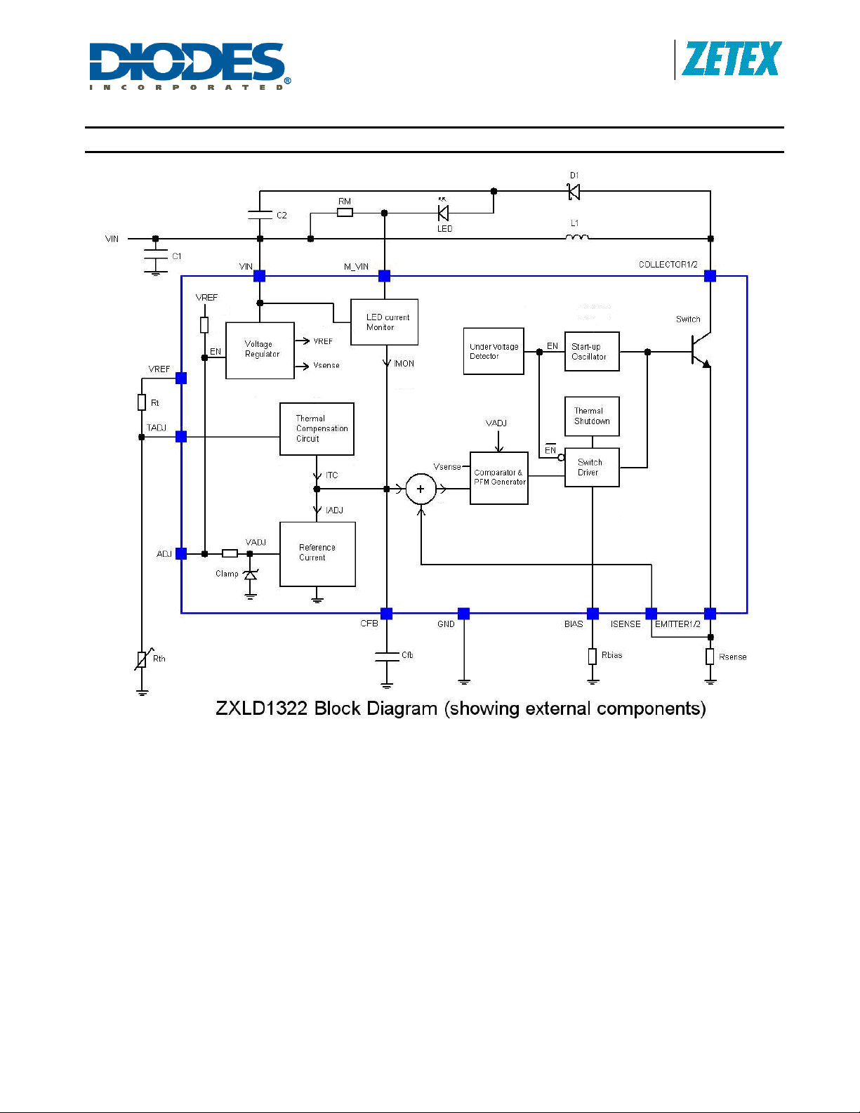
Block Diagram
ZXLD1322
Document number: DS32166 Rev. 3 - 2
2 of 17
www.diodes.com
April 2010
© Diodes Incorporated
A
Product Line o
f
Diodes Incorporated
ZXLD1322
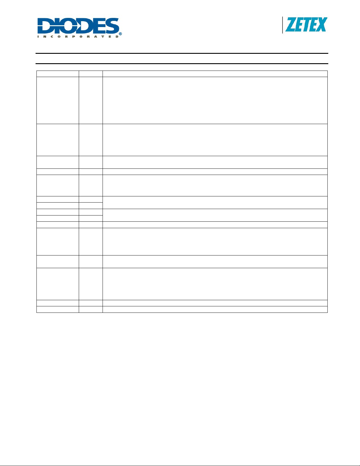
Pin Description
Name Pin # Description
Adjust input
• Leave floating, or connect to V
• Drive with dc voltage. (50mV<V
ADJ 1
of set value. (DC brightness control mode)
• Drive with low frequency (200Hz) PWM control signal to gate output ‘on’ and ‘off’ at
the PWM frequency. (PWM brightness control mode)
• Drive with low level dc voltage (V
Bias pin for setting base current of internal switch transistor
• Short pin to ground to define maximum base drive current for output switch
BIAS 2
(Maximum output current condition)
• Connect resistor (R
) from this pin to ground to reduce base drive current
BIAS
(Reduced output current condition)
CFB 3
Control input/output for feedback control loop
• Connect 10nF capacitor from this pin to ground to provide loop compensation
N/C 4 Not connected internally (Open circuit)
Switch peak current sense pin
ISENSE 5
EMITTER1 6
EMITTER2 7
COLLECTOR2 8
COLLECTOR1 9
• Connect resistor (R
SWPEAK
)=0.05/RS
(I
Switch emitters (Connect both pins to top of RSENSE to sense emitter current)
Switch Collectors (Connect both pins to lower side of coil)
) from this pin to ground to define peak switch current
SENSE
N/C 10 Internally connected - Do not connect to external circuitry
Input supply to high side current monitor
M_VIN 11
VIN 12
• Connect output voltage (whichever is higher)
• Connect resistor (R
current of 0.1/R
) from this pin to to VIN to define nominal average output (LED)
M
M
Input supply voltage and load side input of high side current monitor.
Connect to sensing resistor RM.
Temperature Adjust input for LED thermal compensation
• Connect thermistor/resistor network to this pin to reduce output current above a
TADJ 13
preset temperature threshold.
• Connect to V
to disable thermal compensation function
REF
(see section on temperature control for details)
VREF 14 Internal 0.5V reference voltage output
Exposed Pad 15 Connect to ground (0V)
ZXLD1322
Document number: DS32166 Rev. 3 - 2
3 of 17
www.diodes.com
to set 100% output current.
REF
< V
ADJ
ADJ
) to adjust output current from 10% to 100%
REF
<28mV) to turn off device (Standby mode)
April 2010
© Diodes Incorporated
A
Product Line o
f
Diodes Incorporated
ZXLD1322
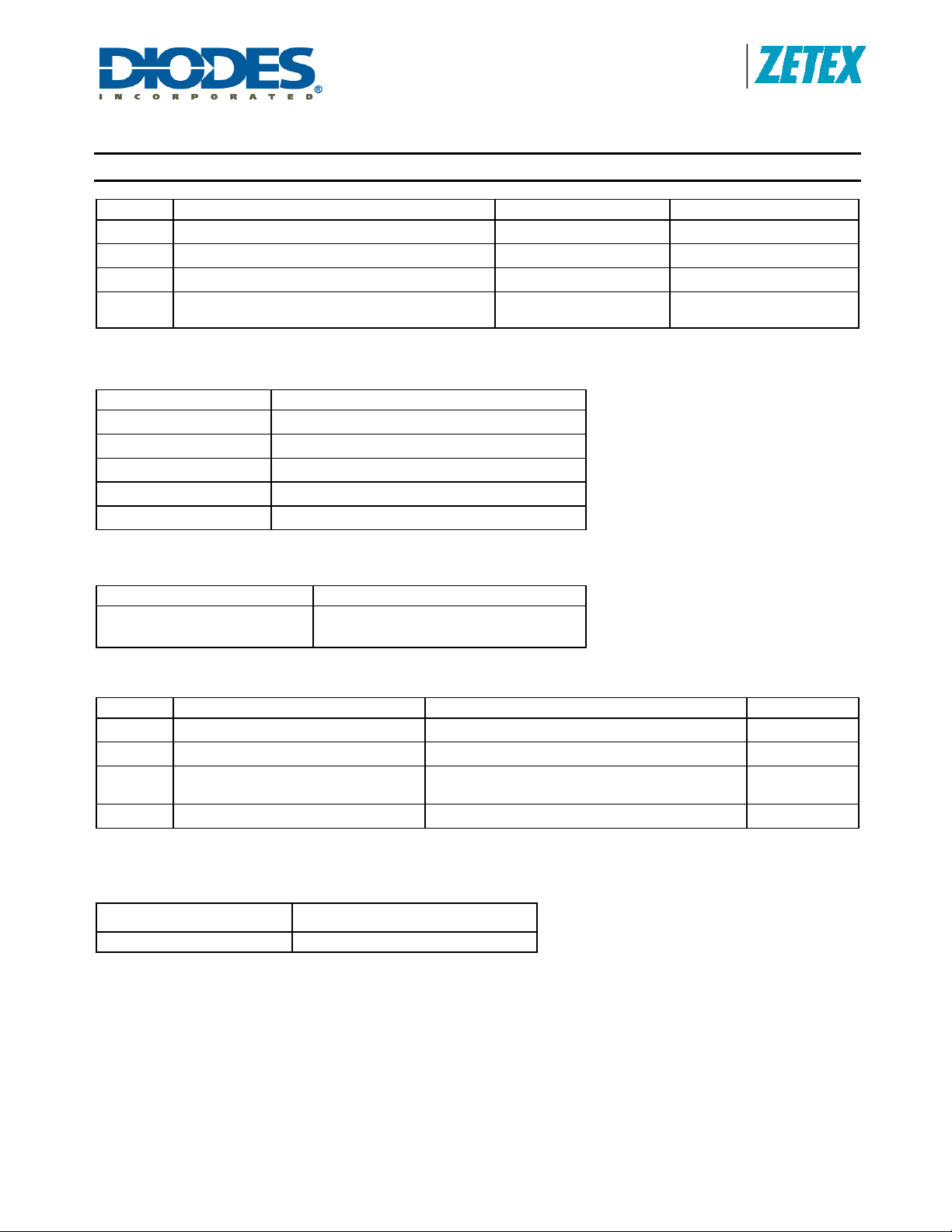
Absolute Maximum Ratings (Voltages to GND Unless Otherwise Stated)
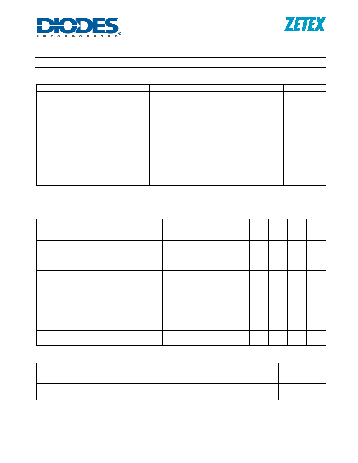
Symbol Parameter Rating Units
TOP
TST
TJ
P
TOT
DC-DC Converter
Supply Voltage (VIN) -0.3V to +15V
High-Side Current Monitor
Monitor Supply Voltage (M_VIN) -0.3V to +15V
Continuous Sense Voltage
(M_V
Switching NPN Transistor
Symbol Parameter Rating Units
V
CBO
V
CEO
ICM
IC
These are stress ratings only. Operation outside the absolute maximum ratings may cause device failure. Operation at the absolute maximum ratings for
extended periods may reduce device reliability.
Thermal Resistance
Junction to ambient (R
DFN4030-14 26.3°C/W
ZXLD1322
Document number: DS32166 Rev. 3 - 2
Operating Temperature -40 to 125 °C
Storage Temperature -55 to 150 °C
Junction Temperature -40 to 150 °C
Package Power Dissipation
DFN14 with Exposed Pad: 4mm x 3mm, 0.5mm Pitch
ADJ
CFB
I
-0.3V to The lower of (+5.0V) or (VIN + 0.3V)
SENSE
T
-0.3V to The lower of (+5.0V) or (VIN + 0.3V)
ADJ
BIAS
– M_LOAD)
IN
Collector-Base Voltage 18 V
Collector-Emitter Voltage 18 V
Peak Pulse Current
Continuous Collector Current
-0.3V to The lower of (+5.0V) or (V
-0.3V to The lower of (+5.0V) or (V
-0.3V to The lower of (+5.0V) or (V
-0.3V to +5V
Nominal Value
)
θJC
(Pulsed Width = 300µs. Duty Cycle<=2%)
4 of 17
www.diodes.com
+ 0.3V)
IN
+ 0.3V)
IN
+ 0.3V)
IN
1.5 at T
=70°C
AMB
3
2 A
W
A
April 2010
© Diodes Incorporated
A
Product Line o
f
Diodes Incorporated
ZXLD1322
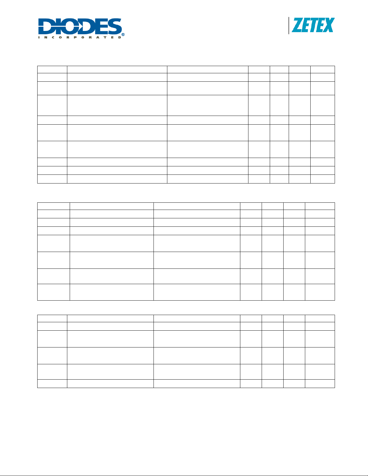
Electrical Characteristics (Test conditions: V
= 4V, T
IN
= 25°C unless otherwise stated
AMB
DC-DC Converter Supply Parameters
Symbol Parameter Condition Min. Typ. Max. Unit
VIN
V
IN(Start)
VUV-
VUV+
Iq Quiescent Current
I
STBY
V
REF
T
CO(REF)
Notes: (a) Production testing of the device is performed at 25°C. Functional operation of the device and parameters specified from -40°C to +125°C are
guaranteed by design, characterization and process control.
(b) Between 1.2V and 2.2V the device will run in the Low Voltage Startup Mode (for details refer to section "Low Voltage Operation")
Supply Voltage Normal Operation 2.5 15 V
Supply voltage for start-up(b) Start-up mode 1.2 2.4 V
Under-voltage detection threshold
normal operation to start-up mode
Under-voltage detection threshold
start-up mode to normal operation
VIN falling 1.8 V
VIN rising 2.2 V
Measured into V
ADJ pin floating.
IN
Excluding switch base current).
Standby Current
Internal Reference Voltage
Internal Reference Temperature
Coefficient
Measured into VIN. ADJ pin grounded
ADJ pin floating
2.5V<V
<15V
IN
DC-DC Converter Input Parameters
Symbol Parameter Condition Min. Typ. Max. Unit
V
SENSE
V
SENSE
(SU)
I
SENSE
CFB
V
ADJ
V
ADJ(th)
T
CO
(V
)
ADJ
R
ADJ
V
ADJ
(CLMP)
Peak switch current sense voltage
Peak switch current sense voltage in
start-up mode
Sense input current
Control loop compensation capacitor 10
External DC control voltage applied to
ADJ pin to adjust output current
Switching threshold of ADJ pin Standby state to normal operation 26 28 30 mV
Temperature coefficient of V
Internal resistor between V
ADJ
Clamp voltage on ADJ pin 100A injected into ADJ pin 575 mV
ADJ(th)
REF
and
Measured on I
SENSE
pin CFB pin
at 0V
Measured on I
SENSE
pin. Start-up
mode VIN = 1.2V
Measured into I
SENSE
with pin at
0V. CFB pin at 0V
DC brightness control mode 50 500 mV
+0.3 %/K
V
<550mV
ADJ
DC-DC Converter Output Parameters
Symbol Parameter Condition Min. Typ. Max. Unit
Toff(100) Discharge pulse width 100% Output current 0.7 1.2 1.7 µs
Toff(10) Discharge pulse width 10% Output current 4 8 12 µs
f
LXMAX
fSU
Maximum operating frequency 600 KHz
Switching frequency in start-up mode VIN = 1.2V 50 KHz
ZXLD1322
Document number: DS32166 Rev. 3 - 2
5 of 17
www.diodes.com
(a)
)
1.5 mA
12 20 µA
480 500 520 mV
50 ppm/K
45 55 65 mV
10.5 mV
-15 -7 -1 µA
100 k
April 2010
© Diodes Incorporated
A
Product Line o
f
Diodes Incorporated
ZXLD1322
Switching NPN Transistor
Symbol Parameter Condition Min. Typ. Max. Unit
ISW
I
BON(max)
Average continuous switch current
Maximum base current into switch
transistor from internal drive circuit
Base current into switch transistor
I
BON
using external resistor (R
BASE
BIAS pin to ground
V
(BR)CE
V
CE(sat)
hFE
C
OBO
Collector-Emitter breakdown voltage
Collector-Emitter saturation voltage
Static forward current transfer ratio
Output capacitance
t(on) Turn-on time
t(off) Turn-off time
High-Side Current Monitor
Symbol Parameter Condition Min. Typ. Max. Unit
V
M_VIN
V
MON
I_
M_VIN
TCO
(MON)
Supply voltage 2.5 18 V
Sense voltage
Input current Measured into M_VIN pin 0.08 1 µA
Temperature coefficient
BW Bandwidth
Gm
ACC
Tran conductance
/VMON
I
OUT
Accuracy
Reference Current Monitor
Symbol Parameter Condition Min. Typ. Max. Unit
V
ADJ
TCO
(MON)
Adjust Voltage 0 500 mV
Temperature coefficient
BW Bandwidth
Gm
ACC
Notes: (c) Measured under pulse conditions.
Tran conductance
/V
I
OUT
ADJ
Accuracy
(d) This current is measured via the collectors and emitters of the switch with these connected to ground (0V)
(e) Measured under pulse conditions. Peak Current = I
ZXLD1322
Document number: DS32166 Rev. 3 - 2
(c)
2 A
30 50 70 mA
10 mA
15 V
50
120
209
116
mV
64 pF
30 ns
28 ns
0 100 200 mV
370
150
350
2.5
ppm/K
KHz
Mhz
) from
(d)
2V<VIN<18V BIAS pin at 0V
R
= 1680
BIAS
IC = 10mA
IC = 0.1A, IB = 10mA
I
= 2A, IB = 50mA
C
IC = 200mA, V
IC = 2A, V
V
CB
CE
= 10V,f = 1MHz
Ic = 0 to IC = 2A V
IC = 2A to Ic < 100A
=V
V
V
V
V
(VIN)
MON
MON
MON
MON
– V
=10mV
=100mV
=10mV
=100mV
M_VIN
CE
= 2V
(e)
= 2V
= 10V
IN
1 mA/V
RM = 0.1
= 100mV
V
MON
= 50mV
V
ADJ
V
= 500mV
ADJ
= 50mV
V
ADJ
V
= 500mV
ADJ
-3 3 %
160
200
275
3
ppm/K
KHz
Mhz
200 µA/V
V
= 500mV
ADJ
C
6 of 17
www.diodes.com
-3 3 %
April 2010
© Diodes Incorporated
 Loading...