

Page 1
A
f
Y
W
Product Line o
Diodes Incorporated
ZXGD3105N8
SYNCHRONOUS MOSFET CONTROLLER IN SO-8
Description
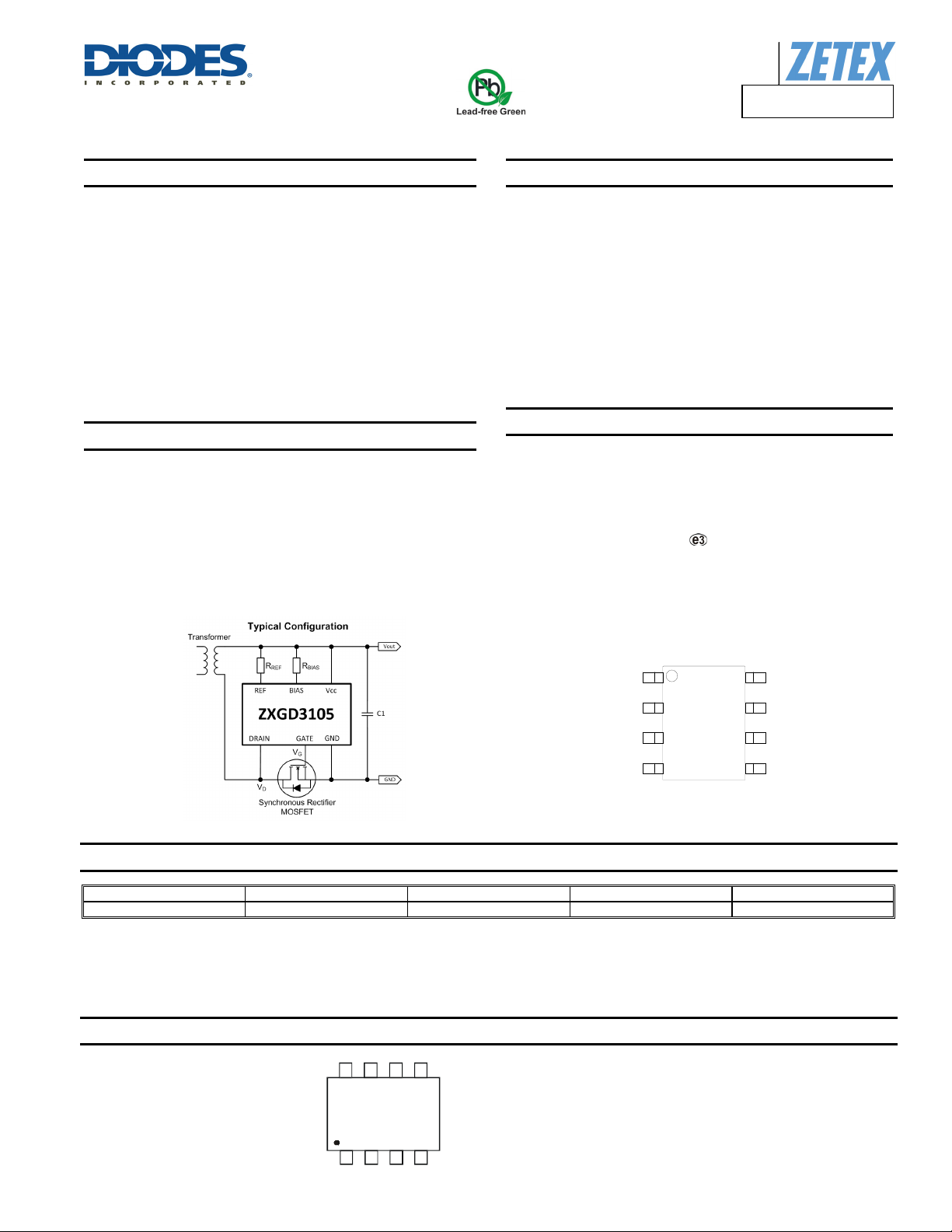
ZXGD3105N8 synchronous controller is designed for driving a
MOSFET as an ideal rectifier. This is to replace a diode for increasing
the power transfer efficiency.
Proportional Gate drive control monitors the reverse voltage of the
MOSFET such that if body diode conduction occurs a positive voltage
is applied to the MOSFET’s Gate pin. Once the positive voltage is
applied to the Gate the MOSFET switches on allowing reverse current
flow. The controllers’ output voltage is then proportional to the
MOSFET Drain-Source voltage and this is applied to the Gate via the
driver. This action minimizes body diode conduction whilst enabling a
rapid MOSFET turn-off as Drain current decays to zero.
Applications
Flyback Converters in:
Low Voltage AC / DC Adaptors
Set Top Box
PoE Power Devices
Resonant Converters in:
Telecoms PSU
Laptop Adaptors
Computing Power Supplies - ATX and Server PSU
Features
Proportional Gate Drive to Minimize Body Diode Conduction
Low Standby Power with Quiescent Supply Current < 1mA
4.5V Operation Enables Low Voltage Supply
25V V
100V Drain Voltage Rating
Operation up to 500kHz
Critical Conduction Mode (CrCM) & Continuous Mode (CCM)
Compliant with Eco-Design Directive
Totally Lead-Free & Fully RoHS compliant (Notes 1 & 2)
Halogen and Antimony free. “Green” Device (Note 3)
Qualified to AEC-Q101 Standards for High Reliability
Rating
CC
Mechanical Data
Case: SO-8
Case material: Molded Plastic. “Green” Molding Compound.
UL Flammability Classification Rating 94V-0
Moisture Sensitivity: Level 1 per J-STD-020
Terminals: Finish – Matte Tin Plated Leads, Solderable per
MIL-STD-202, Method 208
Solderable per MIL-STD-202, Method 208
Weight: 0.074 grams (approximate)
SO-8
Vcc
DNC
BIAS
DRAIN
Top View
Pin-Out
GATE
GND
DNC
REF
Ordering Information (Note 4)
Product Marking Reel size (inches) Tape width (mm) Quantity per reel
ZXGD3105N8TC ZXGD3105 13 12 2500
Notes: 1. No purposely added lead. Fully EU Directive 2002/95/EC (RoHS) & 2011/65/EU (RoHS 2) compliant.
3. Halogen and Antimony free "Green” products are defined as those which contain <900ppm bromine, <900ppm chlorine (<1500ppm total Br + Cl) and
4. For packaging details, go to our website at http://www.diodes.com
2. See http://www.diodes.com for more information about Diodes Incorporated’s definitions of Halogen and Antimony free,"Green" and Lead-Free.
<1000ppm antimony compounds.
Marking Information
ZXGD
3105
Y W
ZXGD3105N8
Document Number DS35101 Rev. 3 - 2
ZXGD = Product Type Marking Code, Line 1
3105 = Product Type Marking Code, Line 2
YY = Year (ex: 11 = 2011)
WW = Week (01 - 53)
1 of 14
www.diodes.com
March 2013
© Diodes Incorporated
Page 2
A
f
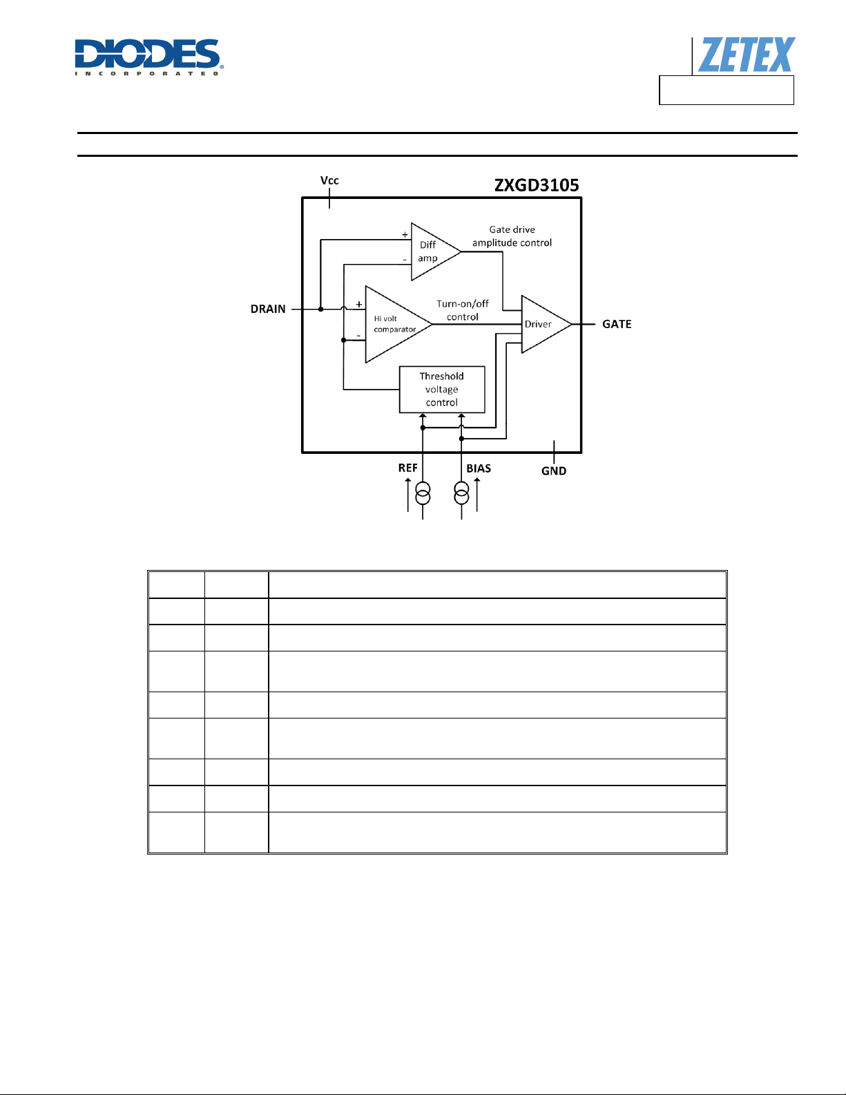
Functional Block Diagram
Product Line o
Diodes Incorporated
ZXGD3105N8
Pin
Number
1
2 DNC
3 BIAS
4 DRAIN
5 REF
6 DNC
7 GND
8 GATE
ZXGD3105N8
Document Number DS35101 Rev. 3 - 2
Pin
Name
V
CC
Description
Power supply
This supply pin should be closely decoupled to ground with a ceramic capacitor.
Do not connect
Leave pin floating.
Bias
Connect this pin to V
Refer to Table 1 and 2, in Application Information section.
Drain sense
Connect directly to the synchronous MOSFET drain terminal.
Reference
Connect this pin to V
Refer to Table 1 and 2, in Application Information section.
Do not connect
Leave pin floating.
Ground
Connect this pin to the synchronous MOSFET source terminal and ground reference point.
Gate drive
This pin sinks and sources the I
gate.
via R
CC
via R
CC
www.diodes.com
resistor. Select R
BIAS
resistor. Select R
REF
SINK
2 of 14
and I
to source 0.54mA into this pin.
BIAS
to source 1.02mA into this pin.
REF
current to the synchronous MOSFET
SOURCE
March 2013
© Diodes Incorporated
Page 3
A
f
Product Line o
Diodes Incorporated
ZXGD3105N8
Maximum Ratings (@T
= +25°C, unless otherwise specified.)
A
Characteristic Symbol Value Unit
Supply voltage, relative to GND
Drain pin voltage
Gate output voltage
Gate Driver peak source current
Gate Driver peak sink current
Reference voltage
Reference current
Bias voltage
Bias current
V
CC
V
D
V
-3 to V
G
I
SOURCE
I
SINK
V
V
REF
I
REF
V
V
BIAS
I
BIAS
25 V
-3 to +100 V
CC
4 A
9 A
CC
25 mA
CC
100 mA
Thermal Characteristics (@T
= +25°C, unless otherwise specified.)
A
Characteristic Symbol Value Unit
490
3.92
655
5.24
720
5.76
785
6.28
255
Power Dissipation
Linear derating factor
Thermal Resistance, Junction to Ambient
(Note 5)
(Note 6)
P
D
(Note 7)
(Note 8)
(Note 5)
(Note 6) 191
(Note 7) 173
R
θJA
(Note 8) 159
Thermal Resistance, Junction to Lead (Note 9) R
Thermal Resistance, Junction to Case (Note 10) R
55 °C/W
θJL
45 °C/W
θJC
Operating Temperature Range TJ -40 to +150
Storage Temperature Range T
-50 to +150
STG
ESD Ratings (Note 11)
+3
V
V
V
mW
mW/°C
°C/W
°C
Characteristic Symbol Value Unit JEDEC Class
Electrostatic Discharge - Human Body Model ESD HBM 4,000 V 3A
Electrostatic Discharge - Machine Model ESD MM 200 V B
Notes: 5. For a device surface mounted on minimum recommended pad layout FR4 PCB with high coverage of single sided 1oz copper, in still air conditions; the
device is measured when operating in a steady-state condition.
6. Same as note (5), except pin 1 (V
7. Same as note (6), except both heatsinks are 10mm x 10mm.
8. Same as note (6), except both heatsinks are 15mm x 15mm.
9. Thermal resistance from junction to solder-point at the end of each lead on pin 1 (V
10. Thermal resistance from junction to top of the case.
11. Refer to JEDEC specification JESD22-A114 and JESD22-A115.
ZXGD3105N8
Document Number DS35101 Rev. 3 - 2
) and pin 7 (GND) are both connected to separate 5mm x 5mm 1oz copper heatsinks.
CC
) or pin 7 (GND).
CC
3 of 14
www.diodes.com
March 2013
© Diodes Incorporated
Page 4
A
f
Thermal Derating Curve
0.8
0.7
0.6
0.5
15mm x 15mm
10mm x 10mm
5mm x 5mm
0.4
Minimum
0.3
Layout
0.2
0.1
0.0
Max Power Dissipation (W)
0 20 40 60 80 100 120 140 160
Junction Temperature (°C)
Derating Curve
Product Line o
Diodes Incorporated
ZXGD3105N8
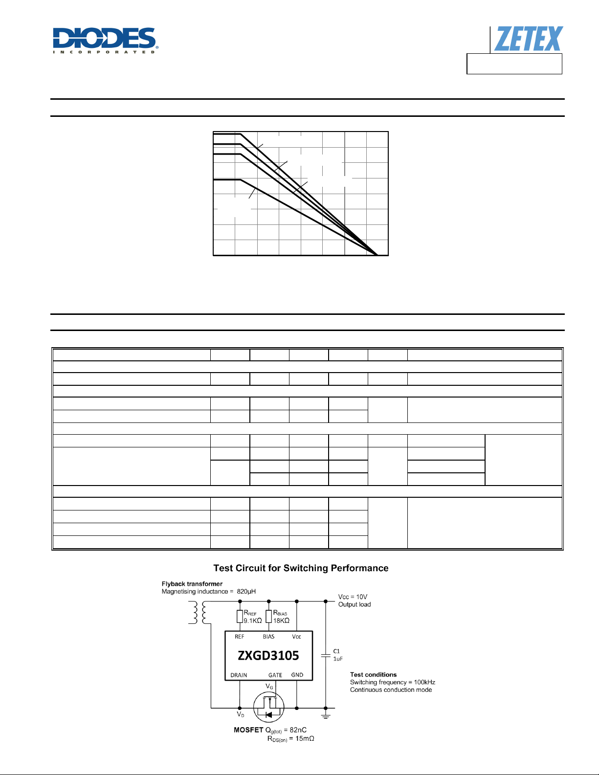
Electrical Characteristics (@T
VCC = 10V; R
Input Supply
Quiescent current
Gate Driver
Gate peak source current
Gate peak sink current
Detector under DC condition
Turn-off Threshold Voltage
Gate output voltage
Switching Performance
Turn-on propagation delay
Gate rise time
Turn-off propagation delay
Gate fall time
BIAS
= 18kΩ (I
= 0.54mA); R
BIAS
Characteristic Symbol Min Typ Max Unit Test Condition
= +25°C, unless otherwise specified.)
A
= 9.1kΩ (I
REF
I
I
SOURCE
I
SINK
V
V
G(off)
VG
t
d(rise)
t
t
d(fall)
t
Q
T
r
f
= 1.02mA)
REF
— 1.56 — mA
— 1.2 —
— 5 —
-20 -10 0 mV
— 0.2 0.6
5.0 7.8 —
8.0 9.4 —
— 118 —
— 77 —
— 14 —
— 26 —
V
≥ 0mV
DRAIN
A
Capacitive load: C
V
= 1V
G
V
≥ 1V
DRAIN
V
V
= -50mV
DRAIN
V
= -100mV
DRAIN
Capacitive load: C
ns
Rise and fall measured 10% to 90%
L
L
= 10nF
Capacitive load only
= 10nF
ZXGD3105N8
Document Number DS35101 Rev. 3 - 2
4 of 14
www.diodes.com
March 2013
© Diodes Incorporated
Page 5
A
f
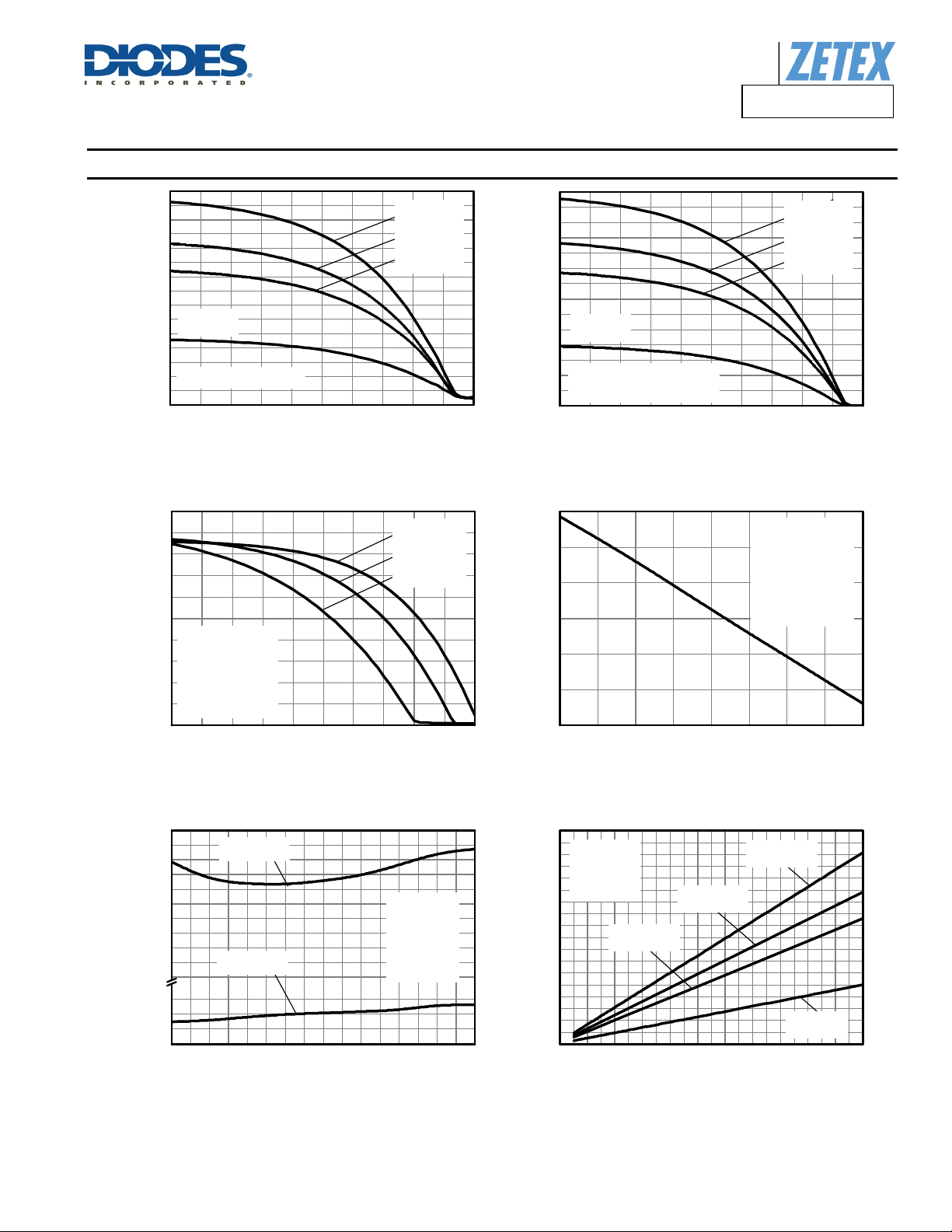
Typical Electrical Characteristics (@T
14
12
10
8
6
VCC = 5V
4
Gate Voltage (V)
G
V
2
Capacitive load only
0
-100 -80 -60 -40 -20 0
VD Drain Voltage (mV)
Transfer Characteristic
= +25°C, unless otherwise specified.)
A
14
VCC = 15V
VCC = 12V
VCC = 10V
12
10
8
6
VCC = 5V
4
Gate Voltage (V)
G
V
Capacitive load and
2
50k pull down resistor
0
-100 -80 -60 -40 -20 0
Product Line o
Diodes Incorporated
ZXGD3105N8
VCC = 15V
VCC = 12V
VCC = 10V
VD Drain Voltage (mV)
Transfer Characteristic
10
Ta = -40°C
8
Ta = 25°C
Ta = 125°C
6
4
VCC = 10V
R
=18k
Gate Voltage (V)
G
V
BIAS
2
R
REF
50k pull down
=9.1k
0
-100 -80 -60 -40 -20 0
VD Drain Voltage (mV)
Transfer Characteristic
230
220
210
200
190
180
170
160
150
140
130
45
40
Switching Time (ns)
35
30
-50 -25 0 25 50 75 100 125 150
Ton = td1 + t
T
off
= td2 + t
r
f
Temperature (°C)
VCC = 10V
R
R
CL=10nF
BIAS
REF
=18k
=9.1k
0
VCC = 10V
-5
-10
-15
R
=18k
BIAS
R
=9.1k
REF
VG = 1V
50k pull down
-20
Drain Voltage (mV)
-25
D
V
-30
-50 0 50 100 150
Temperature (°C)
Drain Sense Voltage vs Temperature
180
R
160
140
120
100
=18k
BIAS
R
=9.1k
REF
f=500kHz
VCC = 12V
VCC = 10V
80
60
40
Supply Current (mA)
20
0
0 2 4 6 8 10 12 14 16 18 20 22
Capacitance (nF)
VCC = 15V
VCC = 5V
Switching vs Temperature
ZXGD3105N8
Document Number DS35101 Rev. 3 - 2
5 of 14
www.diodes.com
Supply Current vs Capacitive Load
March 2013
© Diodes Incorporated
Page 6

A
f
Typical Electrical Characteristics (cont.) (@T
10
= +25°C, unless otherwise specified.)
A
Diodes Incorporated
10
Product Line o
ZXGD3105N8
8
V
6
D
4
2
Voltage (V)
0
-2
-100 0 100 200 300
V
G
VCC=10V
R
=18k
BIAS
R
=9.1k
REF
CL=10nF
RL=0R1
8
6
4
2
Voltage (V)
0
-2
-200 -100 0 100 200 300
Time (ns)
Switch On Speed
4
Ton = td1 + t
r
2
0
Time (ns)
100
10
T
= td2 + t
off
f
VCC=10V
R
=18k
BIAS
R
=9.1k
REF
RL=0R1
-2
-4
-6
Gate Drive Current (A)
-8
110100
Capacitance (nF)
Switching vs Capacitive Load
VCC=10V
R
V
D
V
G
BIAS
R
REF
CL=10nF
RL=0R1
Time (ns)
Switch Off Speed
I
sourc e
VCC=10V
R
=18k
BIAS
R
=9.1k
REF
CL=10nF
RL=0R1
I
sink
0 200 400 600
Time (ns)
Gate Drive Current
=18k
=9.1k
8
6
4
2
VCC=10V
R
=18k
BIAS
R
=9.1k
REF
RL=0R1
-I
sink
I
sourc e
100
10
VCC=10V
R
=18k
BIAS
R
=9.1k
REF
RL=0R1
CL=100nF
CL=33nF
CL=10nF
CL=3.3nF
CL=1nF
Supply Current (mA)
Peak Drive Current (A)
0
110100
Capacitance (nF)
Gate Current vs Capacitive Load
ZXGD3105N8
Document Number DS35101 Rev. 3 - 2
6 of 14
www.diodes.com
1
10 100 1000 10000 100000
Frequency (Hz)
Supply Current vs Frequency
© Diodes Incorporated
March 2013
Page 7

A
f
Product Line o
Diodes Incorporated
ZXGD3105N8
Application Information
The purpose of the ZXGD3105 is to drive a MOSFET as a low-VF Schottky diode replacement in isolated AC/DC converter. When combined with
a low R
minimal component count. Figure 1 shows the typical configuration of ZXGD3105 for synchronous rectification in a low output voltage Flyback
converter.
A typical circuit configuration of synchronous rectification with ZXGD3105 for use in resonant converter is shown in Figure 2. Two ZXGD3105
together with two synchronous MOSFETs should be used on the secondary side of the center tapped transformer winding.
MOSFET, the controller can yield significant power efficiency improvement, whilst maintaining design simplicity and incurring
DS(ON)
Figure 1 Typical Flyback application schematic
Figure 2 Synchronous rectification in resonant converter
Threshold Voltage and Resistor Setting
The correct selection of external resistors R
and I
I
REF
recommended I
pin of the controller. I
BIAS
REF
and I
are 1.02mA and 0.54mA respectively.
BIAS
The values for R
REF
and R
are selected based on the VCC voltage. If the VCC pin is connected to the power converter’s output, the resistors
BIAS
should be selected based on the nominal converter’s output voltage. Table 1 provides the recommended resistor values for different Vcc voltages.
Supply, V
(V)
5 9.6 4.3
10 18 9.1
12 24 11
15 30 15
REF
REF
and I
CC
and R
BIAS
is important for optimum device operation. R
BIAS
combines to set the turn-off threshold voltage level, VT. In order to set VT to -10mV, the
Bias Resistor, R
BIAS
Reference Resistor, R
(kΩ)
Table 1 Recommended resistor values for different VCC voltages
REF
and R
(kΩ)
supply fixed current into the
BIAS
REF
ZXGD3105N8
Document Number DS35101 Rev. 3 - 2
7 of 14
www.diodes.com
March 2013
© Diodes Incorporated
Page 8

A
f
Product Line o
Diodes Incorporated
Application Information (cont.)
Functional Descriptions for Flyback Converter
The operation of the device is described step-by-step with reference to the timing diagram in Figure 3.
1. The detector stage monitors the MOSFET Drain-Source voltage.
2. When, due to transformer action, the MOSFET body diode is forced to conduct there is a negative voltage on the Drain pin due to the
body diode forward voltage.
3. As the negative Drain voltage crosses the turn-off Threshold voltage V
ground after the turn-on delay time t
GATE pin.
4. The controller goes into proportional gate drive control — the GATE output voltage is proportional to the MOSFET on-resistance-
induced Drain-Source voltage. Proportional gate drive ensures that MOSFET conducts during the majority of the conduction cycle to
minimize power loss in the body diode.
5. As the Drain current decays linearly toward zero, proportional gate drive control reduces the Gate voltage so the MOSFET can be
turned off rapidly at zero current crossing. The GATE voltage falls to 1V when the Drain-Source voltage crosses the detection
threshold voltage to minimize reverse current flow.
6. At zero Drain current, the controller GATE output voltage is pulled low to V
. This voltage is then fed to the MOSFET driver stage and current is sourced out of the
d(fall)
, the detector stage outputs a positive voltage with respect to
T
to ensure that the MOSFET is off.
G(off)
ZXGD3105N8
Figure 3 Timing diagram for a critical conduction mode Flyback converter
ZXGD3105N8
Document Number DS35101 Rev. 3 - 2
8 of 14
www.diodes.com
March 2013
© Diodes Incorporated
Page 9

A
f
Application Information (cont.)
Functional Descriptions for Resonant Converter
The operation of the ZXGD3105 in resonant converter is described with reference to Figure 4.
1. The detector stage monitors the MOSFET Drain-GND voltage.
2. When, due to transformer action, the MOSFET body diode is forced to conduct there is a negative voltage on the Drain pin due to the
body diode forward voltage.
3. As the negative Drain voltage crosses the Threshold voltage V
after the turn-on delay time t
4. The controller goes into Proportional Gate Drive control. The GATE voltage now varies according to the MOSFET’s Drain-GND
voltage. During this phase, the relationship of V
the Drain current decays linearly, the Gate voltage reduces so the MOSFET can be turned off rapidly at zero current crossing.
Proportional Gate Drive also ensures that gate voltage is supplied to the MOSFET gate until the Drain current is virtually zero. This
eliminates any parasitic diode conduction after the MOSFET switches off.
5. The GATE voltage falls to 1V when the Drain-GND voltage reaches V
current goes to zero, with little or no reverse current. Threshold voltage V
voltage V
6. At zero Drain current, the GATE voltage is pulled low to V
is 1V (refer to electrical characteristic section in page 4).
G
. This voltage is then fed to the MOSFET driver stage and current is sourced out of the GATE pin.
d(rise)
vs. VD is shown by the transfer characteristic curve in page xx of this datasheet. As
G
, the detector stage outputs a positive voltage with respect to ground
T
. The MOSFET is turned off precisely when the sinusoidal
T
is defined as the Drain voltage VD level at which Gate
T
to ensure that the MOSFET is off.
G(off)
Product Line o
Diodes Incorporated
ZXGD3105N8
Figure 4 Timing diagram of synchronous rectification in the resonant converter
ZXGD3105N8
Document Number DS35101 Rev. 3 - 2
9 of 14
www.diodes.com
March 2013
© Diodes Incorporated
Page 10

A
f
Product Line o
Diodes Incorporated
ZXGD3105N8
Application Information (cont.)
Besides that, Proportional Gate Drive improves the rectifier efficiency even at light to medium load condition by ensuring that the MOSFETs
conduct during majority of the conduction cycle as shown in Figure 5a.
At reduced load condition, early termination of the gate drive voltage is likely for digital level gate drive due to the low current, which means that
the threshold V
This is shown by an increase in Drain-GND voltage for the remaining time of the current waveform. With the current flowing through the body
diode there will be an increase in power developed within the MOSFET. The efficiency impact due to early termination of digital level gate driver
increases with lower R
is breached. With the early termination of the gate drive voltage, MOSFET turns off and the body diode conducts, see Figure 5.
T
MOSFET and/or higher operating frequency.
DS(on)
(a)
Figure 5 Timing diagram of synchronous rectification in the resonant converter
(a) Proportional Gate Drive and (b) Digital Level Gate Drive
ZXGD3105N8
Document Number DS35101 Rev. 3 - 2
(b)
10 of 14
www.diodes.com
March 2013
© Diodes Incorporated
Page 11

A
f
Product Line o
Diodes Incorporated
ZXGD3105N8
Application Information (cont.)
Gate Driver
The controller is provided with single channel high current gate drive output, capable of driving one or more N-channel power MOSFETs. The
controller can operate from Vcc of 4.5V to drive both standard MOSFETs and logic level MOSFETs.
The Gate pins should be as close to the MOSFET’s gate as possible. A resistor in series with GATE pin helps to control the rise time and
decrease switching losses due to gate voltage oscillation. A diode in parallel to the resistor is typically used to maintain fast discharge of the
MOSFET’s gate.
Figure 6 Typical connection of the ZXGD3105 to the synchronous MOSFET
Quiescent Current Consumption
The quiescent current consumption of the controller is the sum of I
consumption, I
I
also controls the gate driver peak sink current whilst I
REF
1.02mA and 0.54mA, the gate driver is able to provide 2A source and 6A sink current. The gate current decreases if I
Care must be taken in reducing the controller quiescent current so that sufficient drive current is still delivered to the MOSFET particularly for high
switching frequency application.
and I
REF
Bias Current, I
(mA)
0.25 0.61 39.2 15.4 0.86
0.35 0.81 28.0 11.5 1.16
0.46 0.99 21.5 9.3 1.45
0.50 1.00 19.6 8.9 1.50
0.55 1.13 17.8 8.1 1.68
0.80 1.66 12.1 5.6 2.46
can be further reduced by increasing the value of resistor R
BIAS
BIAS
Ref Current, I
Table 2 Quiescent current consumption for different resistor values at VCC = 10V
REF
(mA)
Bias Resistor, R
controls the peak source current. At the default current value of I
BIAS
REF
(kΩ)
and I
. For an application that requires ultra-low standby power
BIAS
BIAS
and R
REF
Ref Resistor, R
BIAS
(kΩ)
.
REF
Quiescent Current, I
(mA)
REF
REF
and I
are reduced.
BIAS
Q
and I
BIAS
of
ZXGD3105N8
Document Number DS35101 Rev. 3 - 2
11 of 14
www.diodes.com
March 2013
© Diodes Incorporated
Page 12

A
f
Product Line o
Diodes Incorporated
ZXGD3105N8
Application Information (cont.)
Layout Guidelines
When laying out the PCB, care must be taken in decoupling the ZXGD3105 closely to VCC and ground with 1μF low-ESR, low-ESL X7R type
ceramic bypass capacitor. If the converter’s output voltage is higher than 20V, a 12V zener diode should be connected from the bias pin to GND to
clamp the Gate voltage and protect the synchronous MOSFET. Figure 7 shows the typical connection diagram.
Figure 7 Zener Voltage Clamp Arrangement
GND is the ground reference for the internal high voltage amplifier as well as the current return for the gate driver. So the ground return loop
should be as short as possible. Sufficient PCB copper area should be allocated to the Vcc and GND pin for heat dissipation especially for high
switching frequency application.
Any stray inductance involved by the load current may cause distortion of the drain-to-source voltage waveform, leading to premature turn-off of
the synchronous MOSFET. In order to avoid this issue, drain voltage sensing should be done as physically close to the drain terminals as
possible. The PCB track length between the controller Drain pin and the MOSFET’s terminal should be kept less than 10mm. MOSFET packages
with low internal wire bond inductance are preferred for high switching frequency power conversion to minimize body diode conduction.
After the primary MOSFET turns off, its Drain voltage oscillates due to reverse recovery of the snubber diode. These high frequency oscillations
are reflected across the transformer to the Drain terminal of the synchronous MOSFET. The synchronous controller senses the Drain voltage
ringing, causing its gate output voltage to oscillate. The synchronous MOSFET cannot be fully enhanced until the Drain voltage stabilizes.
In order to prevent this issue, the oscillations on the primary MOSFET can be damped with either a series resistor Rd to the snubber diode or an
R-C network across the diode (refer Figure 8). Both methods reduce the oscillations by softening the snubber diode’s reverse recovery
characteristic.
Figure 8 Primary Side Snubber Network to Reduce Drain Voltage Oscillations
ZXGD3105N8
Document Number DS35101 Rev. 3 - 2
12 of 14
www.diodes.com
March 2013
© Diodes Incorporated
Page 13

A
f
Package Outline Dimensions
Please see AP02002 at http://www.diodes.com/datasheets/ap02002.pdf for latest version.
e
D
E1
E
A1
Detail ‘A’
h
°
45
A2
A3
A
b
L
0.254
Gauge Plan e
Seating Plane
7°~9
°
Detail ‘A’
Suggested Pad Layout
Please see AP02001 at http://www.diodes.com/datasheets/ap02001.pdf for the latest version.
X
Dimensions Value (in mm)
X 0.60
C1
C2
Y
Y 1.55
C1 5.4
C2 1.27
Product Line o
Diodes Incorporated
Dim Min Max
SO-8
A - 1.75
A1 0.10 0.20
A2 1.30 1.50
A3 0.15 0.25
b 0.3 0.5
D 4.85 4.95
E 5.90 6.10
E1 3.85 3.95
e 1.27 Typ
h - 0.35
L 0.62 0.82
0 8
All Dimensions in mm
ZXGD3105N8
ZXGD3105N8
Document Number DS35101 Rev. 3 - 2
13 of 14
www.diodes.com
March 2013
© Diodes Incorporated
Page 14

A
f
Product Line o
IMPORTANT NOTICE
DIODES INCORPORATED MAKES NO WARRANTY OF ANY KIND, EXPRESS OR IMPLIED, WITH REGARDS TO THIS DOCUMENT,
INCLUDING, BUT NOT LIMITED TO, THE IMPLIED WARRANTIES OF MERCHANTABILITY AND FITNESS FOR A PARTICULAR PURPOSE
(AND THEIR EQUIVALENTS UNDER THE LAWS OF ANY JURISDICTION).
Diodes Incorporated and its subsidiaries reserve the right to make modifications, enhancements, improvements, corrections or other changes
without further notice to this document and any product described herein. Diodes Incorporated does not assume any liability arising out of the
application or use of this document or any product described herein; neither does Diodes Incorporated convey any license under its patent or
trademark rights, nor the rights of others. Any Customer or user of this document or products described herein in such applications shall assume
all risks of such use and will agree to hold Diodes Incorporated and all the companies whose products are represented on Diodes Incorporated
website, harmless against all damages.
Diodes Incorporated does not warrant or accept any liability whatsoever in respect of any products purchased through unauthorized sales channel.
Should Customers purchase or use Diodes Incorporated products for any unintended or unauthorized application, Customers shall indemnify and
hold Diodes Incorporated and its representatives harmless against all claims, damages, expenses, and attorney fees arising out of, directly or
indirectly, any claim of personal injury or death associated with such unintended or unauthorized application.
Products described herein may be covered by one or more United States, international or foreign patents pending. Product names and markings
noted herein may also be covered by one or more United States, international or foreign trademarks.
This document is written in English but may be translated into multiple languages for reference. Only the English version of this document is the
final and determinative format released by Diodes Incorporated.
LIFE SUPPORT
Diodes Incorporated products are specifically not authorized for use as critical components in life support devices or systems without the express
written approval of the Chief Executive Officer of Diodes Incorporated. As used herein:
A. Life support devices or systems are devices or systems which:
1. are intended to implant into the body, or
2. support or sustain life and whose failure to perform when properly used in accordance with instructions for use provided in the
labeling can be reasonably expected to result in significant injury to the user.
B. A critical component is any component in a life support device or system whose failure to perform can be reasonably expected to cause the
failure of the life support device or to affect its safety or effectiveness.
Customers represent that they have all necessary expertise in the safety and regulatory ramifications of their life support devices or systems, and
acknowledge and agree that they are solely responsible for all legal, regulatory and safety-related requirements concerning their products and any
use of Diodes Incorporated products in such safety-critical, life support devices or systems, notwithstanding any devices- or systems-related
information or support that may be provided by Diodes Incorporated. Further, Customers must fully indemnify Diodes Incorporated and its
representatives against any damages arising out of the use of Diodes Incorporated products in such safety-critical, life support devices or systems.
Copyright © 2013, Diodes Incorporated
www.diodes.com
Diodes Incorporated
ZXGD3105N8
ZXGD3105N8
Document Number DS35101 Rev. 3 - 2
14 of 14
www.diodes.com
March 2013
© Diodes Incorporated
 Loading...