

Page 1
A
f
Y
W
Product Line o
Diodes Incorporated
ZXGD3104N8
SYNCHRONOUS MOSFET CONTROLLER IN SO8
Features
• 5-25V Vcc range
• Operating up to 250kHz
• Suitable for Discontinuous Mode (DCM), Critical Conduction
Mode (CrCM) and Continuous Mode (CCM) operation
• Turn-off propagation delay 15ns and turn-off time 20ns.
• Proportional Gate Drive
• Detector threshold voltage -10mV
• Standby current 5mA
• “Lead-Free”, RoHS Compliant (Note 1)
• Halogen and Antimony free. “Green” Device (Note 2)
• Qualified to AEC-Q101 Standards for High Reliability
Mechanical Data
• Case: SO-8
• Case material: Molded Plastic. “Green” Molding Compound.
• UL Flammability Rating 94V-0
• Moisture Sensitivity: Level 1 per J-STD-020
• Terminals: Matte Tin Finish
• Solderable per MIL-STD-202, Method 208
• Weight: 0.074 grams (approximate)
SO-8
DRAINDNC
REF
GATEL
GATEH
Top View
Pin-Out
BIAS
GND
V
CC
Description
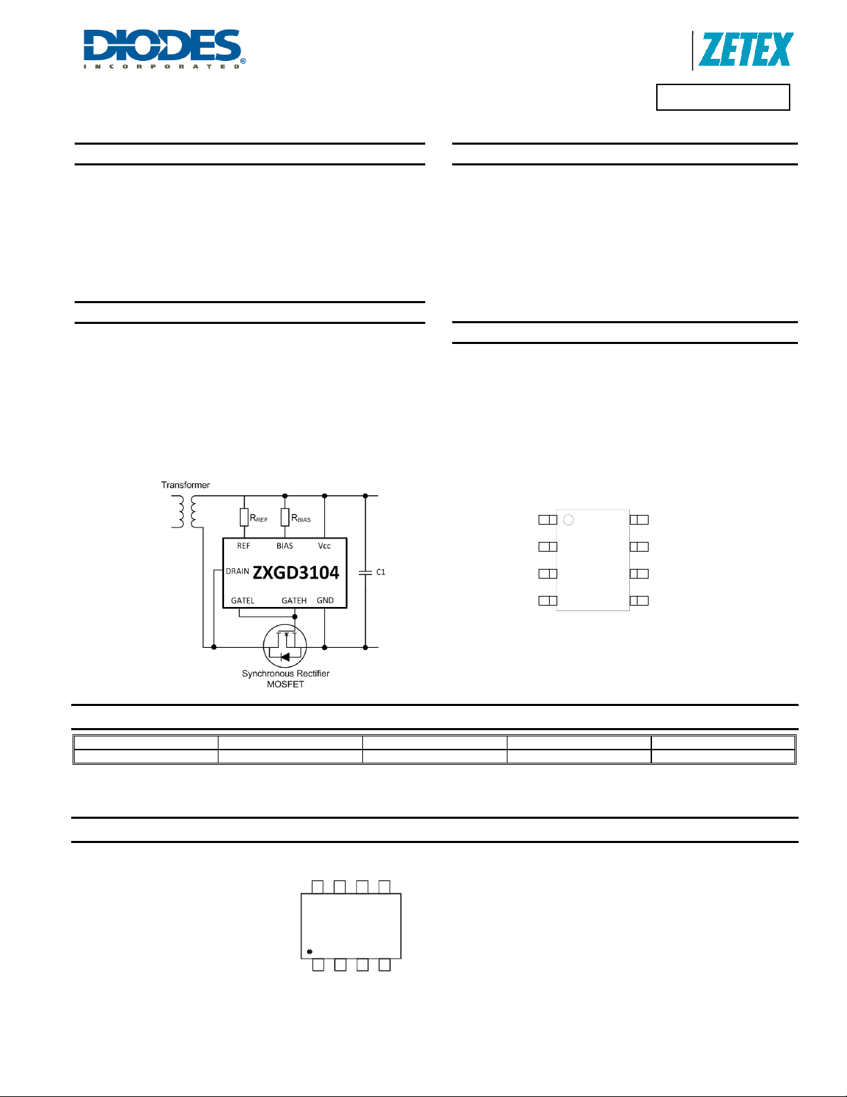
The ZXGD3104 is intended to drive MOSFETS configured as ideal
diode replacements. The device is comprised of a differential amplifier
detector stage and high current driver. The detector monitors the
reverse voltage of the MOSFET such that if body diode conduction
occurs a positive voltage is applied to the MOSFET’s Gate pin.
Once the positive voltage is applied to the Gate the MOSFET switches
on. The detectors’ output voltage is then proportional to the MOSFET
Drain-Source voltage and this is applied to the Gate via the driver.
This action provides a rapid MOSFET turn off at zero Drain current.
Applications
• Flyback Converters in:
o 90W Laptop Adaptors
Typical Configuration
Ordering Information (Note 3)
Product Marking Reel size (inches) Tape width (mm) Quantity per reel
ZXGD3104N8TC ZXGD3104 13 12 2,500
Notes: 1. No purposefully added lead
2. Diodes Inc’s “Green” Policy can be found on our website at http://www.diodes.com
3. For packaging details, go to our website at http://www.diodes.com
Marking Information
ZXGD = Product Type Marking Code, Line 1
3104 = Product Type Marking Code, Line 2
YY = Year (ex: 11 = 2011)
WW = Week (01 - 53)
1 of 13
November 2011
© Diodes Incorporated
ZXGD3104N8
Document Number DS35546 Rev. 1 – 2
ZXGD
3104
Y W
www.diodes.com
Page 2
A
f
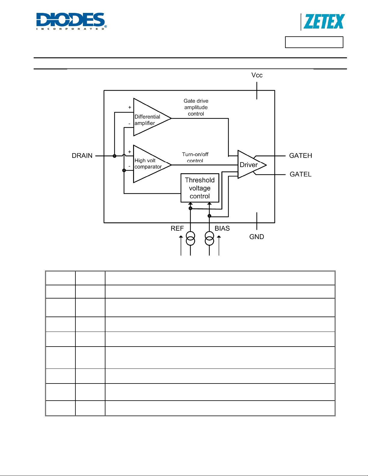
Functional Block Diagram
Product Line o
Diodes Incorporated
ZXGD3104N8
Pin No. Name Description and function
1 DNC
2 REF
3 GATEL
4 GATEH
5 VCC
6 GND
7 BIAS
8 DRAIN
Do not connect
Leave pin floating.
Reference
This pin is connected to VCC via resistor, R
1, in Application Information section.
Gate turn off
This pin sinks current, I
Gate turn on
This pin sources current, I
Power Supply
This is the supply pin. It is recommended to decouple this point to ground closely with a ceramic
capacitor.
Ground
This is the ground reference point. Connect to the synchronous MOSFET Source terminal.
Bias
This pin is connected to V
in Application Information section.
Drain connection
This pin connects directly to the synchronous MOSFET Drain terminal.
Select R
REF.
, from the synchronous MOSFET Gate.
SINK
, to the synchronous MOSFET Gate.
SOURCE
via resistor, R
CC
BIAS.
Select R
to source 2.16mA into this pin. Refer to Table
REF
BIAS
to source 3mA into this pin. Refer to Table 1,
ZXGD3104N8
Document Number DS35546 Rev. 1 – 2
2 of 13
www.diodes.com
November 2011
© Diodes Incorporated
Page 3
A
f
Product Line o
Diodes Incorporated
ZXGD3104N8
Maximum Ratings @T
= 25°C unless otherwise specified
A
Characteristic Symbol Value Unit
Supply voltage, relative to GND VCC 25 V
Drain pin voltage VD -3 to 180 V
Gate output voltage VG -3 to V
Gate Driver peak source current I
Gate Driver peak sink current I
Reference voltage V
Reference current I
Bias voltage V
Bias current I
2.5 A
SOURCE
7 A
SINK
V
REF
25 mA
REF
V
BIAS
100 mA
BIAS
+ 3 V
CC
V
CC
V
CC
Thermal Characteristics @T
= 25°C unless otherwise specified
A
Characteristic Symbol Value Unit
490
3.92
655
5.24
720
5.76
785
6.28
255
mW
mW/°C
°C/W
Power Dissipation
Linear derating factor
Thermal Resistance, Junction to Ambient
(Note 4)
(Note 5)
P
(Note 6)
D
(Note 7)
(Note 4)
(Note 5) 191
(Note 6) 173
R
JA
(Note 7) 159
Thermal Resistance, Junction to Lead (Note 8)
Operating Temperature Range
Storage Temperature Range
Notes: 4. For a device surface mounted on minimum recommended pad layout FR4 PCB with high coverage of single sided 1oz copper, in still air conditions; the
device is measured when operating in a steady-state condition.
5. Same as note (4), except pin 5 (V
6. Same as note (5), except both heatsinks are 10mm x 10mm.
7. Same as note (5), except both heatsinks are 15mm x 15mm.
8. Thermal resistance from junction to solder-point at the end of each lead on pin 5 (V
) and pin 6 (GND) are both connected to separate 5mm x 5mm 1oz copper heatsinks.
CC
R
JL
T
J
T
STG
) and pin 6 (GND).
CC
135
-40 to +150
-50 to +150
°C/W
°C
ZXGD3104N8
Document Number DS35546 Rev. 1 – 2
3 of 13
www.diodes.com
November 2011
© Diodes Incorporated
Page 4
A
f
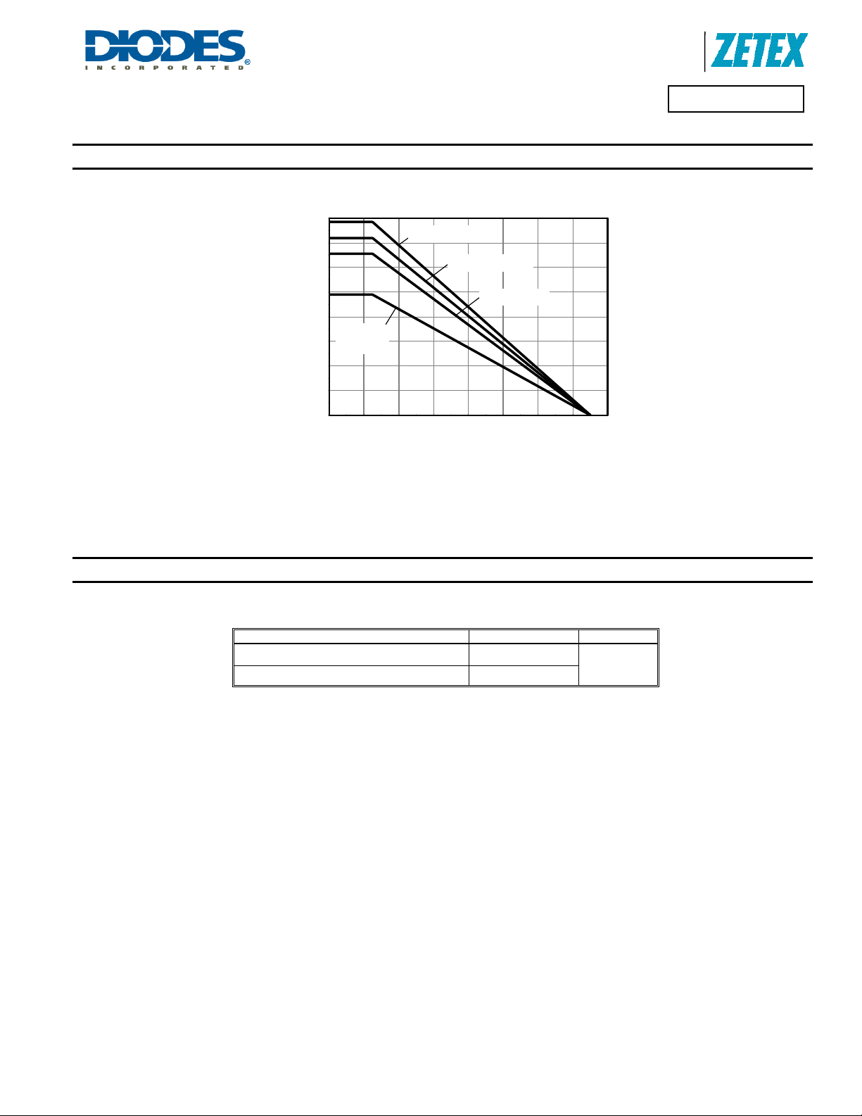
Thermal Derating Curve
0.8
0.7
0.6
Product Line o
Diodes Incorporated
ZXGD3104N8
15mm x 15mm
10mm x 10mm
ESD Rating
0.5
0.4
Minimum
0.3
Layout
0.2
0.1
0.0
Max Powe r Di ssi p at ion (W)
0 20 40 60 80 100 120 140 160
5mm x 5mm
Junction Temperatu re (°C)
Derating Curve
Characteristic Value Unit
ESD for Human Body Model 2000
ESD for Machine Model 300
V
ZXGD3104N8
Document Number DS35546 Rev. 1 – 2
4 of 13
www.diodes.com
November 2011
© Diodes Incorporated
Page 5

A
f
)
Product Line o
Diodes Incorporated
ZXGD3104N8
Electrical Characteristics @T
= 25°C unless otherwise specified
A
V
= 19V; R
CC
= 6.3kΩ; R
BIAS
= 8.5kΩ
REF
Characteristic Symbol Min Typ Max Unit Test Condition
Input and Supply
Quiescent current IQ - 5.16 - mA V
Gate Driver
Turn-off Threshold Voltage (Note 9 & 10) VT -16 -10 0 mV V
0 0.73 1.0 V V
G(off
12.5 14 V
17 18
V
V
CC
Gate output voltage
(Note 9 & 10) V
(Note 9 & 11) VG
Switching Performance for QG(tot) = 124nC (Note 12)
Turn-on propagation delay
Turn-off propagation delay
Gate rise time
Gate fall time
t
d(rise)
t
d(fall)
t
t
r
f
175 250 325
11 15 20
335 480 625 From 10% of VG to 10V
ns
530 760 990 From 10% to 90% of VG
35 50 65 Continuous Conduction Mode
Notes: 9.GATEH connected to GATEL
10.R
= 100k, RL = O/C
H
11.R
= 100k, RH = O/C
L
12. refer to test circuit below
0V
D
= 1V
G
1V
D
= -50mV
D
= -100mV
V
D
Refer to switching
waveforms in Fig. 1
ZXGD3104N8
Document Number DS35546 Rev. 1 – 2
5 of 13
www.diodes.com
November 2011
© Diodes Incorporated
Page 6

A
f
Product Line o
Diodes Incorporated
ZXGD3104N8
Descriptions of the normal operation
The operation of the controller is described step-by-step with reference to the timing diagram in Figure 1.
1. The controller monitors the MOSFET Drain-Source voltage.
2. When, due to transformer action, the MOSFET body diode is forced to conduct there is approximately -0.8V on the
Drain pin.
3. The detector outputs a positive voltage with respect to ground, this voltage is then fed to the MOSFET driver stage
and current is sourced out of the GATE pin.
4. The controller goes into proportional gate drive control — the GATE output voltage is proportional to the onresistance-induced Drain-Source voltage drop across the MOSFET. Proportional gate drive ensures that MOSFET
conducts for majority of the conduction cycle and minimizes body diode conduction time.
5. As the Drain current decays linearly toward zero, proportional gate drive control reduces the Gate voltage so the
MOSFET can be turned off rapidly at zero current crossing. The GATE voltage is removed when the Drain-Source
voltage crosses the detection threshold voltage to minimize reverse current flow.
6. At zero Drain current, the controller GATE output voltage is pulled low to V
to ensure that the MOSFET is off.
G(off)
Figure 1. Timing diagram for a critical conduction mode Flyback converter
ZXGD3104N8
Document Number DS35546 Rev. 1 – 2
6 of 13
www.diodes.com
November 2011
© Diodes Incorporated
Page 7

A
f
Typical Electrical Characteristics @T
= 25°C unless otherwise specified
A
Product Line o
Diodes Incorporated
ZXGD3104N8
ZXGD3104N8
Document Number DS35546 Rev. 1 – 2
7 of 13
www.diodes.com
November 2011
© Diodes Incorporated
Page 8

A
f
Continued - Typical Electrical Characteristics @T
Product Line o
Diodes Incorporated
= 25°C unless otherwise specified
A
ZXGD3104N8
ZXGD3104N8
Document Number DS35546 Rev. 1 – 2
8 of 13
www.diodes.com
November 2011
© Diodes Incorporated
Page 9

A
f
Product Line o
Diodes Incorporated
ZXGD3104N8
Application Information
The purpose of the ZXGD3104 is to drive a MOSFET as a low-V
converters. When combined with a low R
MOSFET, it can yield significant power efficiency improvement, whilst
DS(ON)
maintaining design simplicity and incurring minimal component count. Figure 2 shows typical configuration of
ZXGD3104 for synchronous rectification in a 19V output Flyback Adaptor.
Schottky diode replacement in offline power
F
Figure 2. Example connections in Flyback power supply
Figure 3 shows operating waveforms for ZXGD3104 driving a MOSFET with Q
converter operating in critical conduction mode.
= 124nC in a 19V output Flyback
g(TOT)
ZXGD3104N8
Document Number DS35546 Rev. 1 – 2
9 of 13
www.diodes.com
November 2011
© Diodes Incorporated
Page 10

A
f
Product Line o
Diodes Incorporated
Typical waveforms
Fig 3a: Critical conduction mode, operating for MOSFET with Q
ZXGD3104N8
=124nC
g(TOT)
Fig 3b: Typical switching waveform
Fig 3c: Close up of typical turn off waveform
ZXGD3104N8
Document Number DS35546 Rev. 1 – 2
10 of 13
www.diodes.com
November 2011
© Diodes Incorporated
Page 11

A
f
Product Line o
Diodes Incorporated
ZXGD3104N8
Design considerations
It is advisable to decouple the ZXGD3104 closely to VCC and ground due to the possibility of high peak gate currents
with a 1F X7R type ceramic capacitor C1 as shown in Figure 2. Also the ground return loop should be as short as
possible.
To minimize parasitic inductance-induced premature turn-off of the synchronous controller always keep the PCB
track length between ZXGD3104’s Drain input and MOSFET’s Drain to less than 10mm. Low internal inductance
SMD MOSFET packages are also recommended for high switching frequency power conversion to minimize
MOSFET body diode conduction loss.
The Gate pins should be as close to the MOSFET’s gate as possible. External gate resistors are optional. They can
be inserted to control the rise and fall time which may help with EMI issues.
The careful selection of external resistors R
for resistor R
REF
and R
from Table 1 based on the desired Vcc value. This provides the typical ZXGD3104’s
BIAS
REF
and R
is important to the optimum device operation. Select a value
BIAS
detection threshold voltage of -10mV.
Table 1. Recommended resistor values for various supply voltages
VCC R
5V
10V
12V
15V
19V
R
BIAS
1.6
k 2 k
3.3
k 4.3 k
3.9
k 5.1 k
5.1
k 6.8 k
6.3
k 8.5 k
REF
ZXGD3104N8
Document Number DS35546 Rev. 1 – 2
11 of 13
www.diodes.com
November 2011
© Diodes Incorporated
Page 12

A
f
0
Package Outline Dimensions
DIM Inches Millimeters DIM Inches Millimeters
Product Line o
Diodes Incorporated
ZXGD3104N8
hx45°
Min. Max. Min. Max. Min. Max. Min.
A 0.053 0.069 1.35 1.75 e 0.050 BSC 1.27 BSC
A1 0.004 0.010 0.10 0.25 b 0.013 0.020 0.33 0.51
D 0.189 0.197 4.80 5.00 c 0.008 0.010 0.19 0.25
H 0.228 0.244 5.80 6.20
E 0.150 0.157 3.80 4.00 h 0.010 0.020 0.25 0.50
L 0.016 0.050 0.40 1.27 - - - - -
Suggested Pad Layout
0.6
.024
7.0
0.275
Max.
θ
0° 8° 0° 8°
1.52
0.060
4.0
0.155
1.27
0.050
mm
inches
ZXGD3104N8
Document Number DS35546 Rev. 1 – 2
12 of 13
www.diodes.com
November 2011
© Diodes Incorporated
Page 13

A
f
Product Line o
Diodes Incorporated
ZXGD3104N8
DIODES INCORPORATED MAKES NO WARRANTY OF ANY KIND, EXPRESS OR IMPLIED, WITH REGARDS TO THIS DOCUMENT,
INCLUDING, BUT NOT LIMITED TO, THE IMPLIED WARRANTIES OF MERCHANTABILITY AND FITNESS FOR A PARTICULAR PURPOSE
(AND THEIR EQUIVALENTS UNDER THE LAWS OF ANY JURISDICTION).
Diodes Incorporated and its subsidiaries reserve the right to make modifications, enhancements, improvements, corrections or other changes
without further notice to this document and any product described herein. Diodes Incorporated does not assume any liability arising out of the
application or use of this document or any product described herein; neither does Diodes Incorporated convey any license under its patent or
trademark rights, nor the rights of others. Any Customer or user of this document o r products described herein in such applica tions shall assume
all risks of such use and will agree to hold Diodes Incorporated and all the companies whose products are represented on Diodes Incorporated
website, harmless against all damages.
Diodes Incorporated does not warrant or accept any liability whatsoever in respect of any products purchased through unauthorized sales channel.
Should Customers purchase or use Diodes Incorporated products for any unintended or unauthorize d application, Customers shall indemnify and
hold Diodes Incorporated and its representatives harmless against all claims, damages, expenses, and attorney fees arising out of, directly or
indirectly, any claim of personal injury or death associated with such unintended or unauthorized application.
Products described herein may be covered by one or more United States, international or foreign patents pending. Product names and markings
noted herein may also be covered by one or more United States, international or foreign trademarks.
Diodes Incorporated products are specifically not authorized for use as critical components in life support devices or systems without the express
written approval of the Chief Executive Officer of Diodes Incorporated. As used herein:
A. Life support devices or systems are devices or systems which:
1. are intended to implant into the body, or
2. support or sustain life and whose failure to perform when properly used in accordance with instructions for use provided in the
labeling can be reasonably expected to result in significant injury to the user.
B. A critical component is any component in a life support device or system whose failure to perform can be reasonably expected to cause the
failure of the life support device or to affect its safety or effectiveness.
Customers represent that they have all necessary expertise in the safety and regulatory ramifications of their life support devices or systems, and
acknowledge and agree that they are solely responsible for all legal, regulatory and safety-related requirements concerning their products and any
use of Diodes Incorporated products in such safety-critical, life support devices or systems, notwithstanding any devices- or systems-related
information or support that may be provided by Diodes Incorporated. Further, Customers must fully indemnify Diodes Incorporated and its
representatives against any damages arising out of the use of Diodes Incorporated products in such safety-critical, life support devices or systems.
Copyright © 2011, Diodes Incorporated
www.diodes.com
IMPORTANT NOTICE
LIFE SUPPORT
ZXGD3104N8
Document Number DS35546 Rev. 1 – 2
13 of 13
www.diodes.com
November 2011
© Diodes Incorporated
 Loading...