

Page 1
A
f
Y
W
Product Line o
Diodes Incorporated
ZXGD3103N8
SYNCHRONOUS MOSFET CONTROLLER
Description
The ZXGD3103 is intended to drive MOSFETS
configured as ideal diode replacements. The
device is comprised of a differential amplifier
detector stage and high current driver. The
detector monitors the reverse voltage of the
MOSFET such that if body diode conduction
occurs a positive voltage is applied to the
MOSFET’s Gate pin.
Features
• Proportional Gate Drive
• Turn-off propagation delay 15ns and turn-off
time 20ns.
• Detector threshold voltage ~10mV
• Standby current 5mA
• Suitable for Discontinuous Mode (DCM),
Critical Conduction Mode (CrCM) and
Continuous Mode (CCM) operation
• 5-15V V
range
CC
Once the positive voltage is applied to the Gate
the MOSFET switches on allowing reverse current
flow. The detectors’ output voltage is then
proportional to the MOSFET Drain-Source reverse
voltage drop and this is applied to the Gate via the
driver. This action provides a rapid turn off as
current decays.
Applications
• Flyback Converters in:
• Adaptors
• LCD Monitors
• Server PSU’s
• Set Top Boxes
• LCD TV
• Resonant Converters
• LED TV
• High power Adaptors
• Street Lighting
• ATX psu
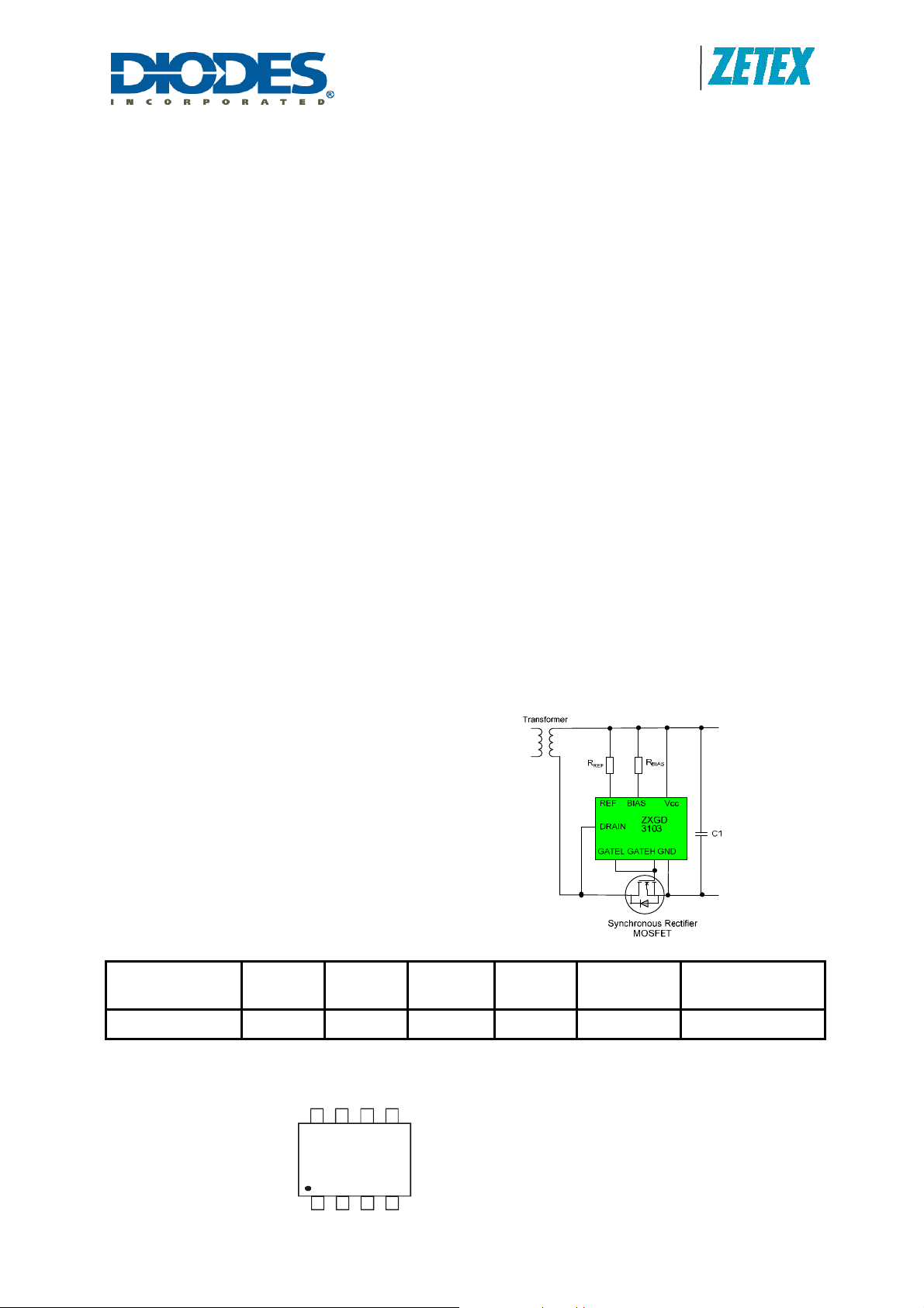
Pin out details
Typical Configuration
SO-8
Ordering information
Device Status Package Part Mark
Reel size
(inches)
Tape width
(mm)
Quantity per reel
ZXGD3103N8TC Production SO8 ZXGD3103 13 12 2500
Marking information
ZXGD
3103
Y W
ZXGD = Product Type Marking Code, Line 1
3103 = Product Type Marking Code, Line 2
YY = Year (ex: 11 = 2011)
WW = Week (01 - 53)
ZXGD3103N8
Document number: DS32255 Rev. 2 - 2
1 of 12
www.diodes.com
November 2011
© Diodes Incorporated
Page 2
A
f
Product Line o
Diodes Incorporated
ZXGD3103N8
Absolute maximum ratings
Parameter Symbol Limit Unit
Supply voltage1 V
Continuous Drain pin voltage1 V
GATEH and GATEL output Voltage1 V
Driver peak source current I
Driver peak sink current I
Reference current I
Bias voltage V
Bias current I
Power dissipation at TA =25°C
15 V
CC
-3 to180 V
D
-3 to V
G
2.5 A
SOURCE
6 A
SINK
25 mA
REF
V
BIAS
100 mA
BIAS
P
490 mW
D
+ 3 V
CC
V
CC
Operating junction temperature Tj -40 to +150
Storage temperature T
Notes: 1. All voltages are relative to GND pin.
-50 to +150
stg
Thermal resistance
°C
°C
Parameter Symbol Value Unit
Junction to ambient (a) R
Junction to lead (b) R
Notes: a. Mounted on minimum 1oz weight copper on FR4 PCB in still air conditions.
b. Output Drivers - Junction to solder point at end of the lead 5 and 6
255 °C/W
θJA
120 °C/W
θlA
ESD Rating
Model Rating Unit
Human Body 2000 V
Machine 300 V
ZXGD3103N8
Document number: DS32255 Rev. 2 - 2
2 of 12
www.diodes.com
November 2011
© Diodes Incorporated
Page 3
A
f
Product Line o
Diodes Incorporated
ZXGD3103N8
Electrical characteristics at TA = 25°C; VCC = 10V; R
Parameter Symbol Conditions Min. Typ. Max. Unit
Input and supply characteristics
≤ -200m V - 2.16 -
V
Operating current IOP
Gate Driver
Turn-off Threshold
Voltage(**)
V
T
V
G(off)
GATE output voltage (**)
VG
D
VD ≥ 0V - 5.16 -
V
= 1V, (*)
G
V
≥ 0V, (*)
D
= -50mV, (g)
V
D
VD = -100mV, (g)
VD ≤ -150mV, (g)
= 3.3kΩ; R
BIAS
= 4.3kΩ
REF
mA
-16 -10 0 mV
- 0.73 1
6.0 7.2 -
8.8 9.2 -
V
9.2 9.4 -
VD ≤ -200mV, (g)
9.3 9.5 -
Switching performance (“) for QG(tot) = 82nC
Turn on Propagation delay t
Turn off Propagation delay td2 15
d1
Refer to switching waveforms
in Fig. 3
150
Gate rise time tr 450
Gate fall time tf
Notes:
(**) GATEH connected to GATEL
(*) R
= 100kΩ, RL = O/C
H
= 100kΩ, RH = O/C
(g) R
L
Continuous Conduction Mode
Discontinuous Conduction
Mode
21
17
(“) refer to test circuit below
ns
ZXGD3103N8
Document number: DS32255 Rev. 2 - 2
3 of 12
www.diodes.com
November 2011
© Diodes Incorporated
Page 4
A
f
Product Line o
Diodes Incorporated
ZXGD3103N8
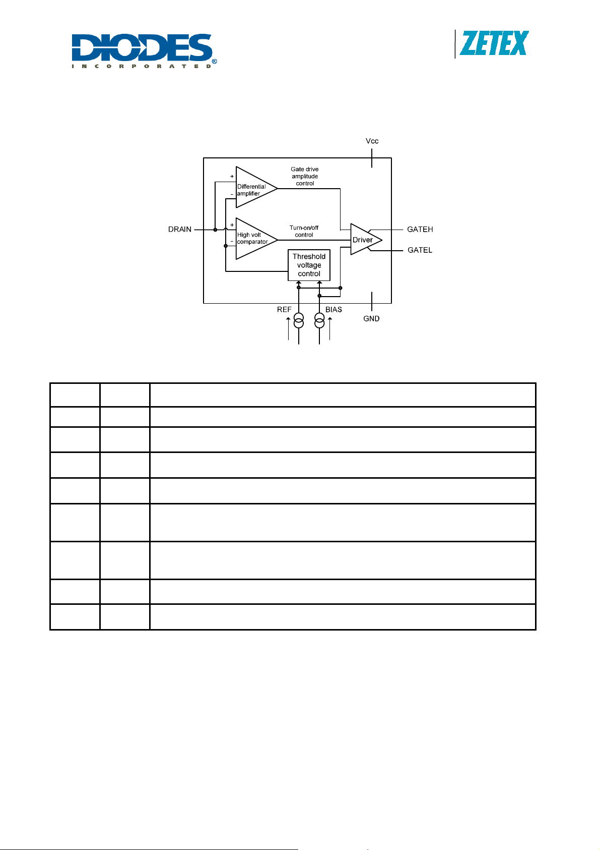
Schematic Symbol and Pin Out Details
Pin No. Name Description and function
1
2
3 GATEL
4
NC No Internal connection
REF
Reference
This pin is connected to V
Gate turn off
GATEH
This pin sinks current, I
Gate turn on
This pin sources current, I
SINK
Power Supply
5 VCC
This is the supply pin. It is recommended to decouple this point to ground closely
with a ceramic capacitor.
Ground
6 GND
This is the ground reference point. Connect to the synchronous MOSFET Source
terminal.
7 BIAS
8
DRAIN
Bias
This pin is connected to V
Drain connection
This pin connects directly to the synchronous MOSFET Drain terminal.
via resistor, R
CC
REF
, from the synchronous MOSFET Gate.
, to the synchronous MOSFET Gate.
SOURCE
via resistor, R
CC
BIAS
.
ZXGD3103N8
Document number: DS32255 Rev. 2 - 2
4 of 12
www.diodes.com
November 2011
© Diodes Incorporated
Page 5

A
f
Product Line o
Diodes Incorporated
ZXGD3103N8
Typical Characteristics
14
12
10
8
6
4
Gate Voltage (V)
G
V
2
See Resistor Table for Values
0
-100 -80 -60 -40 -20 0
VD Drain Voltage (mV)
Transfer Characteristic
5
0
-5
-10
-15
VCC = 10V
R
R
VG = 1V
100k pull up
VCC = 15V
VCC = 12V
VCC = 10V
VCC = 5V
=3K3
BIAS
=4K3
REF
10
8
6
4
VCC = 10V
R
=3K3
Gate Voltage (V)
G
V
BIAS
2
R
=4K3
REF
100k pull down
0
-100 -80 -60 -40 -20 0
VD Drain Voltage (mV)
Transfer Characteristic
100
10
VCC = 10V
R
=3k3
BIAS
R
=4K3
REF
D = 0.5
C
=22nF
LOAD
C
=10nF
LOAD
C
=4.7nF
LOAD
C
=2.2nF
LOAD
C
=1nF
LOAD
T = -40°C
T = 25°C
T = 85°C
T = 125°C
Drain Voltage (mV )
-20
D
V
-25
-50 -25 0 25 50 75 100 125 150
Temperature (°C)
Drain Sense Voltage vs Temperature
100
R
=3k3
BIAS
R
80
60
40
20
=4K3
REF
D = 0.5
f=250kHz
Supply Current (mA )
0
0 2 4 6 8 10 12 14 16 18 20 22
VCC = 15V
VCC = 12V
VCC = 10V
VCC = 5V
Capacitance (nF)
Supply Current vs Capacitive Load
Supply Current (mA )
1k 10k 100k
Frequency (Hz)
Supply Current vs Frequency
1
0
-1
-2
-3
-4
Peak Current (A)
-5
Current flow Gate to Ground
0 5 10 15 20 25
Current flow Supply to Gate
Capacitance (nF)
Gate Current v s C ap a citive L o ad
VCC = 10V
R
=3K3
BIAS
R
=4K3
REF
T = 2 5°C
ZXGD3103N8
Document number: DS32255 Rev. 2 - 2
5 of 12
www.diodes.com
November 2011
© Diodes Incorporated
Page 6

A
f
Product Line o
Diodes Incorporated
ZXGD3103N8
Typical Characteristics
10
8
6
4
V
D
2
Voltage (V)
VCC=10V
R
V
G
BIAS
R
REF
C
LOAD
0
-2
-0.5 0.0 0.5 1.0 1.5
Time (μs)
Switch On Speed
0.3
0.2
0.1
Gate Current (A)
0.0
-0.5 0.0 0.5 1.0 1.5
Time (μs)
VCC=10V
R
=3k3
BIAS
R
=4K3
REF
C
=10nF
LOAD
Ga te Driv e On Current
=3k3
=4K3
=10nF
10
8
6
4
V
D
2
Voltage (V)
V
G
0
-2
-40 -20 0 20 40 60 80 100 120 140
Time (ns)
Switch Off Speed
2
1
0
-1
-2
Gate Current (A)
-3
-4
-40 -20 0 20 40 60 80 100 120 140
Time (ns)
Gate Drive O ff C u rrent
VCC=10V
R
BIAS
R
=4K7
REF
C
LOAD
VCC=10V
R
=3k3
BIAS
R
=4K3
REF
C
=10nF
LOAD
=10k
=10nF
6
4
VCC=10V
R
BIAS
R
REF
C
LOAD
2
0
-2
Percent Change Time (%)
-50 -25 0 25 50 75 100 125 150
Switching vs Temp erature
ZXGD3103N8
Document number: DS32255 Rev. 2 - 2
=3k3
=4K3
=10nF
tON= tD + t
t
Temperature (°C)
R
= tD + t
OFF
F
www.diodes.com
6 of 12
November 2011
© Diodes Incorporated
Page 7

A
f
Product Line o
Diodes Incorporated
ZXGD3103N8
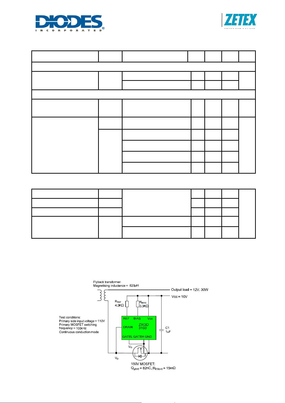
Application information
The purpose of the ZXGD3103 is to drive a MOSFET as a low-VF Schottky diode replacement in offline
power converters. When combined with a low R
improvement, whilst maintaining design simplicity and incurring minimal component count. Figure 1 and 2
show typical configuration of ZXGD3103 for synchronous rectification in a Flyback and a multiple output
resonant converter.
MOSFET, it can yield significant power efficiency
DS(ON)
Figure 1. Example connections in Flyback supply
Figure 2. Example connections in LLC supply
ZXGD3103N8
Document number: DS32255 Rev. 2 - 2
7 of 12
www.diodes.com
November 2011
© Diodes Incorporated
Page 8

A
f
Product Line o
Diodes Incorporated
ZXGD3103N8
Descriptions of the normal operation
The operation of the device is described step-by-step with reference to the timing diagram in Figure 3.
1. The detector monitors the MOSFET Drain-Source voltage.
2. When, due to transformer action, the MOSFET body diode is forced to conduct there is approximately -
0.8V on the Drain pin.
3. The detector outputs a positive voltage with respect to ground, this voltage is then fed to the MOSFET
driver stage and current is sourced out of the GATE pin.
4. The controller goes into proportional gate drive control — the GATE output voltage is proportional to the
on-resistance-induced Drain-Source voltage drop across the MOSFET. Proportional gate drive ensures that
MOSFET conducts for majority of the conduction cycle and minimizes body dio de conduction time.
5. As the Drain current decays linearly toward zero, proportional gate drive control reduces the Gate voltage
so the MOSFET can be turned off rapidly at zero current crossing. The GATE voltage is removed when the
Drain-Source voltage crosses the detection threshold voltage to minimize reverse current flow.
6. At zero Drain current, the controller GATE output voltage is pulled low to V
to ensure that the
G(off)
MOSFET is off.
Figure 4 shows typical operating waveforms for ZXGD3103 driving a MOSFET with Q
Flyback converter operating in critical conduction mode.
= 82nC in a
g(TOT)
Figure 3. Timing diagram for a critical conduction mode Flyback converter
ZXGD3103N8
Document number: DS32255 Rev. 2 - 2
8 of 12
www.diodes.com
November 2011
© Diodes Incorporated
Page 9

A
f
Typical waveforms
Product Line o
Diodes Incorporated
ZXGD3103N8
Fig 4a: Critical conduction mode
Switch O n S peed
10
9
8
7
6
5
4
3
2
Voltage (V)
1
0
-1
-2
V
D
-0.4 -0.2 0.0 0.2 0.4 0.6 0.8 1.0 1.2 1.4 1.6
V
G
VCC = 10V
R
= 3K3
BIAS
= 4K3
R
REF
= 82nC
Q
g(TOT)
Time (μs)
Fig 4b: Typical switch ON speed when driving a Q
Switch O FF S peed
10
9
8
7
6
5
4
3
2
Voltage (V)
1
0
-1
-2
-0.05 -0.04 -0.03 -0.02 -0.01 0.0 0 0.01 0.02 0.03 0.04 0 .05
V
D
Time (μs)
V
G
VCC = 10V
R
= 3K3
BIAS
R
= 4K3
REF
Q
g(TOT)
g(TOT)
= 82nC
= 82nC MOSFET
Fig 4c: Typical switch OFF speed when driving a Q
ZXGD3103N8
Document number: DS32255 Rev. 2 - 2
9 of 12
www.diodes.com
= 82nC MOSFET
g(TOT)
November 2011
© Diodes Incorporated
Page 10

A
f
Product Line o
Diodes Incorporated
ZXGD3103N8
Design considerations
It is advisable to decouple the ZXGD3103 closely to VCC and ground due to the possibility of high peak gate
currents with a 1μF X7R type ceramic capacitor as shown in Figure 2. The Gate pins should be as close to
the MOSFET’s gate as possible. Also the ground return loop should be as short as possible.
To minimize parasitic inductance-induced premature turn-off issue of the synchronous controller always
keep the PCB track length between ZXGD3101’s Drain input and MOSFET’s Drain to less than 10mm. Low
internal inductance MOSFET packages such as SO-8 and PolarPak are also recommended for high
switching frequency power conversion to minimize body diode conduction.
R1, Q1 D1 and C1 in Figure 1 are only required as a series drop-down regulator to maintain a stable Vcc
around 10V from a power supply output voltage greater than 15V.
External gate resistors are optio nal. They can be inserted to control the rise and fall time which may help
with EMI issues.
The proper selection of external resistors R
Select a value for resistor R
typical ZXGD3103’s detection threshold voltage of 10mV.
REF
and R
BIAS
and R
REF
from Table 1 based on the desired Vcc value. This provides the
BIAS
Table 1. Recommended resistor values for various supply voltages
VCC R
5V 1K6 2K0
10V 3K3 4K3
12V 3K9 5K1
15V 5K1 6K8
BIAS
is important to the optimum device operation.
R
REF
ZXGD3103N8
Document number: DS32255 Rev. 2 - 2
10 of 12
www.diodes.com
November 2011
© Diodes Incorporated
Page 11

A
f
Package Outline and Dimensions
Product Line o
Diodes Incorporated
ZXGD3103N8
ZXGD3103N8
Document number: DS32255 Rev. 2 - 2
11 of 12
www.diodes.com
November 2011
© Diodes Incorporated
Page 12

A
f
Product Line o
Diodes Incorporated
ZXGD3103N8
DIODES INCORPORATED MAKES NO WARRANTY OF ANY KIND, EXPRESS OR IMPLIED, WITH REGARDS TO THIS
DOCUMENT, INCLUDING, BUT NOT LIMITED TO, THE IMP LIED WARRANTIES OF MERCHA NTABILITY AND FITNESS
FOR A PARTICULAR PURPOSE (AND THEIR EQUIVALENTS UNDER THE LAWS OF ANY JURISDICTION).
Diodes Incorporated and its subsidiaries reserve the right to make modifications, enhancements, improvements, corrections or
other changes without further notice to this document and any product described herein. Diodes Incorporated does not assume
any liability arising out of the application or use of this document or any product described herein; neither does Diodes
Incorporated convey any license under its patent or trademark rights, nor the rights of others. Any Customer or user of this
document or products described herein in such applications shall assume all risks of such use and will agree to hold Diodes
Incorporated and all the companies whose products are represented on Diodes Incorporated website, harmless against all
damages.
Diodes Incorporated does not warrant or accept any liability whatsoever in respect of any products purchased through
unauthorized sales channel.
Should Customers purchase or use Diodes Incorporated products for any unintended or unauthorized application, Customers
shall indemnify and hold Diodes Incorporated and its representatives harmless against all claims, damages, expenses, and
attorney fees arising out of, directly or indirectly, any claim of personal injury or death associated with such unintended or
unauthorized application.
Products described herein may be covered by one or more United States, international or foreign patents pending. Product
names and markings noted herein may also be covered by one or more United States, international or foreign trademarks.
Diodes Incorporated products are specifically not authorized for use as critical components in life support devices or systems
without the express written approval of the Chief Executive Officer of Diodes Incorporated. As used herein:
A. Life support devices or systems are devices or systems which:
1. are intended to implant into the body, or
2. support or sustain life and whose failure to perform when properly used in accordance with instructions for use
provided in the labeling can be reasonably expected to result in significant injury to the user.
B. A critical component is any component in a life support device or system whose failure to perform can be reasonably
expected to cause the failure of the life support device or to affect its safety or effectiveness.
Customers represent that they have all necessary expertise in the safety and regulatory ramifications of their life support
devices or systems, and acknowledge and agree that they are solely responsible for all legal, regulatory and safety-related
requirements concerning their products and any use of Diodes Incorporated products in such safety-critical, life support devices
or systems, notwithstanding any devices- or systems-related information or support that may be provided by Diodes
Incorporated. Further, Customers must fully indemnify Diodes Incorporated and its representatives against any damages
arising out of the use of Diodes Incorporated products in such safety-critical, life support devices or systems.
Copyright © 2011, Diodes Incorporated
www.diodes.com
IMPORTANT NOTICE
LIFE SUPPORT
ZXGD3103N8
Document number: DS32255 Rev. 2 - 2
12 of 12
www.diodes.com
November 2011
© Diodes Incorporated
 Loading...