Diodes ZXGD3102 User Manual

A
Product Line o
f
Diodes Incorporated
ZXGD3102T8
Description
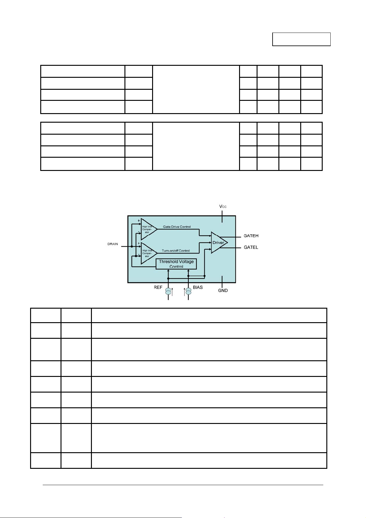
The ZXGD3102 is intended to drive MOSFETs
configured as ideal diode replacements. The
device is comprised of a differential amplifier
detector stage and high current driver. The
detector monitors the reverse voltage of the
MOSFET such that if body diode conduction
occurs a positive voltage is applied to the
MOSFET’s Gate pin.
Features
• Turn-off time typically 105ns
• 180V blocking voltage
• Proportional Gate drive
• 2A Source, 5A Sink driver
• V
Range 5-15V
CC
• Low component count
ACTIVE OR’ING CONTROLLER
Once the positive voltage is applied to the Gate
the MOSFET switches on allowing reverse current
flow. The detectors’ output voltage is then
proportional to the MOSFET Drain-Source reverse
voltage drop and this is applied to the Gate via the
driver. This action provides a rapid turn off as
current decays.
Applications
• High Side OR’ing diode replacement for
Servers, Computer
• Low Side OR’ing diode replacement for
Telecoms
• Ideal diode applications
Pin out details
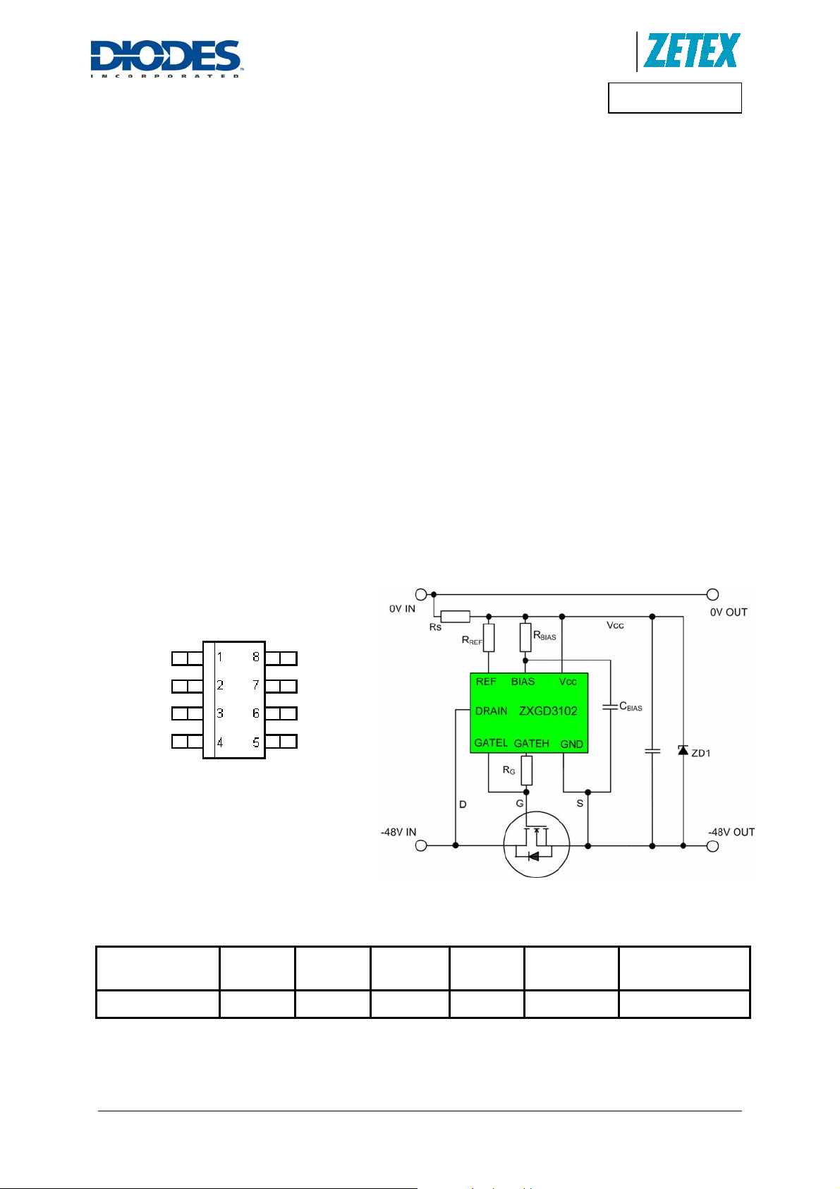
N/C 1
REF 2
GATEL 3
GATEH 4
8 DRAIN
7 BIAS
6 GND
5 VCC
SM8
Ordering information
Device Status Package Part Mark
Typical Configuration
Reel size
(inches)
Tape width
(mm)
Quantity per reel
ZXGD3102T8TA Active SM8 ZXGD3102 7 12 1000
Issue 4, May 2009 1 www.diodes.com
© Diodes Incorporated 2008

ZXGD3102T8
Absolute maximum ratings
Parameter Symbol Limit Unit
Supply voltage1 V
Continuous Drain pin voltage1 V
GATEH and GATEL output Voltage1 V
Driver peak source current I
Driver peak sink current I
Reference current I
Bias voltage V
Bias current I
Power dissipation at TA =25°C
15 V
CC
-3 to180 V
D
-3 to V
G
4 A
SOURCE
7 A
SINK
25 mA
REF
V
BIAS
100 mA
BIAS
P
500 mW
D
+ 3 V
CC
V
CC
Operating junction temperature Tj -40 to +150
Storage temperature T
Notes:
-50 to +150
stg
1. All voltages are relative to GND pin
Thermal resistance
°C
°C
Parameter Symbol Value Unit
Junction to ambient (*) R
Junction to case (†) R
250 °C/W
θJA
54 °C/W
θJC
Notes:
(*) Mounted on minimum 1oz copper on FR4 PCB in still air conditions
(†) Junction to solder point at the end of the lead 5 and 6
ESD Rating
Model Rating Unit
Human body 4,000 V
Machine 400 V
Issue 4, May 2009 2 www.diodes.com
©Diodes Incorporated 2008

ZXGD3102T8
DC Electrical characteristics at T
= 10V; R
V
CC
= 3.3kΩ; R
BIAS
Parameter
=3.9kΩ
REF
= 25°C;
A
Symbol
Input and supply characteristics
Operating current IOP
Gate Driver
Turn-off Threshold Voltage(**)
V
V
G(off)
GATE output voltage (**)
GATEH peak source current I
GATEL peak sink current I
VG
SOURCE
SINK
=3.9kΩ
REF
= 25°C;
A
DC Electrical Characteristics at T
= 10V; R
V
CC
= 3.9kΩ; R
BIAS
T
V
V
Conditions Min. Typ Max. Unit
≤ -100m V - 2.4 -
V
D
VD ≥ 0V - 5.2 -
V
= 1V, (*)
G
V
≥ 0V, (*)
D
= -60mV, (g)
V
D
VD = -80mV, (g)
VD = -100mV, (g)
VD = -140mV, (g)
= 1V 2 - A
GH
= 5V 5 - - A
GL
-50 -24 0 mV
- 0.58 1
4.1 7 -
6.5 8.5 -
8.0 9 -
8.5 9.4 -
mA
V
Parameter
Symbol
Input and supply characteristics
Operating current IOP
Gate Driver
Turn-off Threshold Voltage(**) VT
V
G(off)
GATE output voltage (**)
GATEH peak source current I
GATEL peak sink current I
VG
SOURCE
SINK
Notes:
(**) GATEH connected to GATEL
Conditions Min. Typ Max. Unit
VD ≤ -100m V (g)
VD ≥ 0V (*)
V
= 1V, (*)
G
V
≥ 0V, (*)
D
= -60mV, (g)
V
D
VD = -80mV, (g)
VD = -100mV, (g)
VD = -140mV, (g)
V
V
= 1V 2 - A
GH
= 5V 5 - - A
GL
- 2.4 mA
- 4.8 -
-55 -29 0 mV
- 0.57 1
3.5 6.5 -
6.5 8.5 -
V
8.0 8.8 -
8.5 9.4 -
(*) R
(g) R
= 100kΩ, RL = O/C; RH needed only for characterization purposes, not in the application
H
= 100kΩ, RH = O/C; RL needed only for characterization purposes, not in the application
L
Issue 4, May 2009 3 www.diodes.com
©Diodes Incorporated 2008

ZXGD3102T8
Transient Electrical Characteristics at T
CC = 10V; RBIAS = 3.9k; RREF=3.9k
V
Turn on Propagation delay t
Turn off Propagation delay td2 30 ns
Gate rise time tr 9520 ns
Gate fall time tf 75 ns
d1
= 25°C;
A
= 3.3nF,
C
L
C
BIAS
(g)(a)
1880 ns
= 1nF,
VCC = 10V; RBIAS = 3.9k ; RREF=3.9k
Turn on Propagation delay t
Turn off Propagation delay td2 32 ns
Gate rise time tr 9840 ns
Gate fall time tf 78 ns
d1
= 10nF,
C
L
1940 ns
= 1nF,
C
BIAS
(g)(a)
(a) Refer to Fig 4: test circuit and Fig 5: timing diagram
Schematic Symbol and Pin Out Details
Pin No. Symbol Description and function
1
NC
No connection
This pin can be connected to GND
Reference
2
REF
This pin is connected to V
via resistor, R
CC
REF
source approximately 2.4mA into this pin. See Note 1
3 GATEL
4
GATEH
5 VCC
6 GND
Gate turn off
This pin sinks current, I
, from the OR’ing MOSFET Gate
SINK
Gate turn on
This pin sources current, I
, to the OR’ing MOSFET Gate
SOURCE
Power Supply
This is the supply pin. Decouple this point to ground with a ceramic capacitor
Ground
This is the ground reference point. Connect to the OR’ing MOSFET Source terminal
Bias
7 BIAS
This pin is connected to V
1.2 times I
into this pin depending on the desired turn-off threshold voltage, VT.
REF
CC
via R
BIAS
. R
should be selected to source either 1 or
BIAS
See Note 1
8
DRAIN
Drain connection
This pin connects directly to the OR’ing MOSFET Drain terminal
Note 1- BIAS and REF pins should be assumed to be at GND+0.7V.
. R
should be selected to
REF
Issue 4, May 2009 4 www.diodes.com
©Diodes Incorporated 2008

ZXGD3102T8
Operation
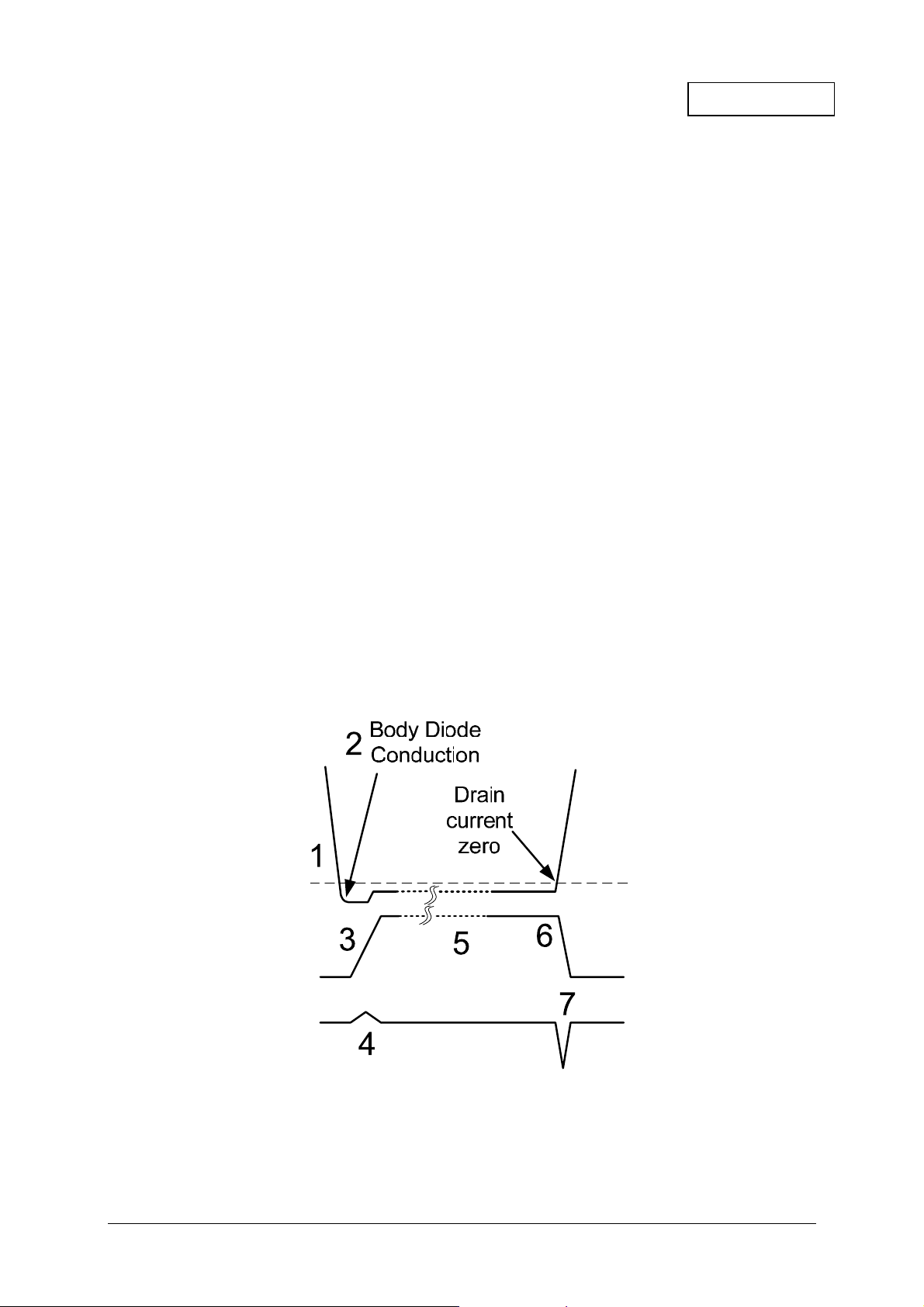
The operation of the device is described step-by-step with reference to the timing diagram below.
1. The detector monitors the MOSFET Drain-Source voltage.
2. At system start up, the MOSFET body diode is forced to conduct current from the input power
supply to the load and there is approximately -0.6V on the Drain pin.
3. The detector outputs a positive voltage with respect to ground, this voltage is then fed to the
MOSFET driver stage and current is sourced out of the GATEH pin. The turn on time of the MOSFET
can be programmed through an external resistor RG. Refer to “Speed vs. Gate resistance” graph.
4. The current out of the GATEH pin is sourced into the OR’ing MOSFET Gate to turn the device on.
5. The GATEH output voltage is proportional to the Drain-Source voltage drop across the MOSFET
due to the load current flowing through the MOSFET. The controller increases its output gate voltage
when the Drain current is high to ensure full MOSFET enhancement
6. If a short condition occurs on the input power supply it causes the OR’ing MOSFET Drain current to
fall very quickly.
7. When the Drain-Source differential voltage drops below the turn off threshold, the MOSFET Gate
voltage is pulled low by GATEL, turning the device off. This prevents high reverse current flow from
the load to the input power supply which could pull down the common bus voltage causing
catastrophic system failure
MOSFET
Drain Voltage
MOSFET
Gate Voltage
MOSFET
Gate Current
Issue 4, May 2009 5 www.diodes.com
©Diodes Incorporated 2008
 Loading...