Diodes ZXGD3101N8 User Manual

A
f
Product Line o
SYNCHRONOUS RECTIFIER CONTROLLER
Description
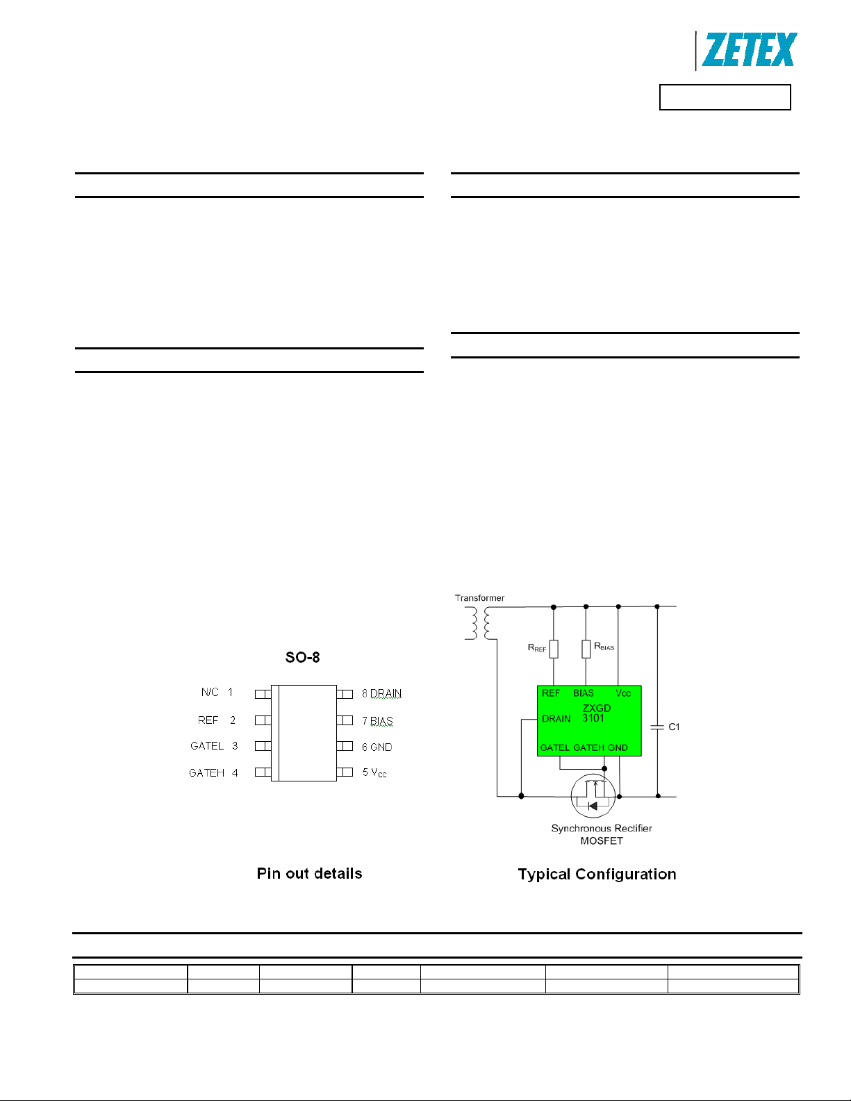
The ZXGD3101 is intended to drive MOSFETS configured as ideal
diode replacements. The device is comprised of a differential amplifier
detector stage and high current driver. The detector monitors the
reverse voltage of the MOSFET such that if body diode conduction
occurs a positive voltage is applied to the MOSFET’s Gate pin.
Once the positive voltage is applied to the Gate the MOSFET
switches on allowing reverse current flow. The detectors’ output
voltage is then proportional to the MOSFET Drain-Source reverse
voltage drop and this is applied to the Gate via the driver. This action
provides a rapid turn off as current decays.
Application
• Flyback Converters in:
• Adaptors
• LCD Monitors
• Server PSU’s
• Set Top Boxes
• LLC Converter in:
• High Power Adaptors
• LCD TV
• Street Lighting
Refer to documents: AN54, AN69, DN90, DN91 and DN94 available
from the website
Features
• Turn-off propagation delay 15ns and turn-off time 20ns.
• Suitable for Discontinuous Mode (DCM), Critical
Conduction Mode (CrCM) and Continuous Mode (CCM)
operation
• Compliant with Energy Star V2.0 and European Code of
Conduct V3
• Halogen Free part
• 5-15V Vcc range
Mechanical Data
• Case: SO-8
• Marking Information: See Page 13
Diodes Incorporated
ZXGD3101N8
Ordering Information
Product Status Package Marking Reel size (inches) Tape width (mm) Quantity per reel
ZXGD3101N8TC Active SO-8 ZXGD3101 13 12 2500
ZXGD3101N8
Document Number DS31945 Rev. 1 - 2
1 of 14
www.diodes.com
June 2010
© Diodes Incorporated

A
f
Product Line o
SYNCHRONOUS RECTIFIER CONTROLLER
Diodes Incorporated
ZXGD3101N8
Maximum Ratings
Parameter Symbol Limit Unit
V
Supply voltage (Note 1)
Continuous Drain pin voltage (Note 1)
GATEH and GATEL output Voltage (Note 1)
Driver peak source current
Driver peak sink current
Reference current
CC
V
D
V
G
I
SOURCE
I
SINK
I
REF
15 V
-3 to180 V
-3 to V
+ 3 V
CC
4 A
7 A
25 mA
V
Bias voltage
Bias current
Power dissipation at TA =25°C
Operating junction temperature
Storage temperature
BIAS
I
BIAS
P
T
T
STG
D
J
-40 to +150 °C
-50 to +150 °C
V
V
CC
100 mA
490 mW
Thermal Characteristics
Parameter Symbol Value Unit
Junction to ambient (Note 2)
Junction to lead (Note 3)
R
JA
R
lA
255 °C/W
120 °C/W
ESD Rating
Model Rating Unit
Human Body 4000 V
Machine 400 V
Notes: 1.All voltages are relative to GND pin
2. Mounted on minimum 1oz weight copper on FR4 PCB in still air conditions.
3. Output Drivers - Junction to solder point at end of the lead 5 and 6
ZXGD3101N8
Document Number DS31945 Rev. 1 - 2
2 of 14
www.diodes.com
June 2010
© Diodes Incorporated

A
f
Product Line o
SYNCHRONOUS RECTIFIER CONTROLLER
Diodes Incorporated
ZXGD3101N8
Electrical Characteristics @T
Parameter Symbol Conditions Min. Typ. Max. Unit
Input and supply characteristics
Operating current
Gate Driver
Turn-off Threshold Voltage(Note 4)
GATE output voltage (Note 4)
GATEH peak source current
= 25°C, VCC= 10V,
A
I
OP
V
V
T
V
G(off)
VG
I
V
SOURCE
=1.8k, R
RBIAS
-200m V
V
DRAIN
V
0V
DRAIN
= 1V, (Note 5)
G
0V, (Note 5)
V
DRAIN
V
= -60mV, (Note 6)
DRAIN
V
= -80mV, (Note 6)
DRAIN
V
= -100mV, (Note 6)
DRAIN
V
-140mV, (Note 6)
DRAIN
V
-200mV, (Note 6)
DRAIN
= 1V
GH
REF
=3k
- 3 mA
- 8 -
-45 -16 0 mV
- 0.6 1
5.0 7.5 -
7.0 8.5 V
8.4 9 -
9.2 9.4 -
9.3 9.5 -
2.5 - A
GATEL peak sink current
Turn on Propagation delay
Turn off Propagation delay
Gate rise time
Gate fall time
Notes: 4. GATEH connected to GATEL
= 100k, RL = O/C
5. R
H
= 100k, RH = O/C
6. R
L
7. Refer to Fig 6: test circuit and Fig 7: timing diagram on Page 12
V
SINK
t
d1
t
d2
t
r
t
f
= 5V
GL
C
= 2.2nF, (Notes 6 and 7)
L
2.5 - A
525 ns
15 ns
305 ns
20 ns
I
ZXGD3101N8
Document Number DS31945 Rev. 1 - 2
3 of 14
www.diodes.com
June 2010
© Diodes Incorporated

A
f
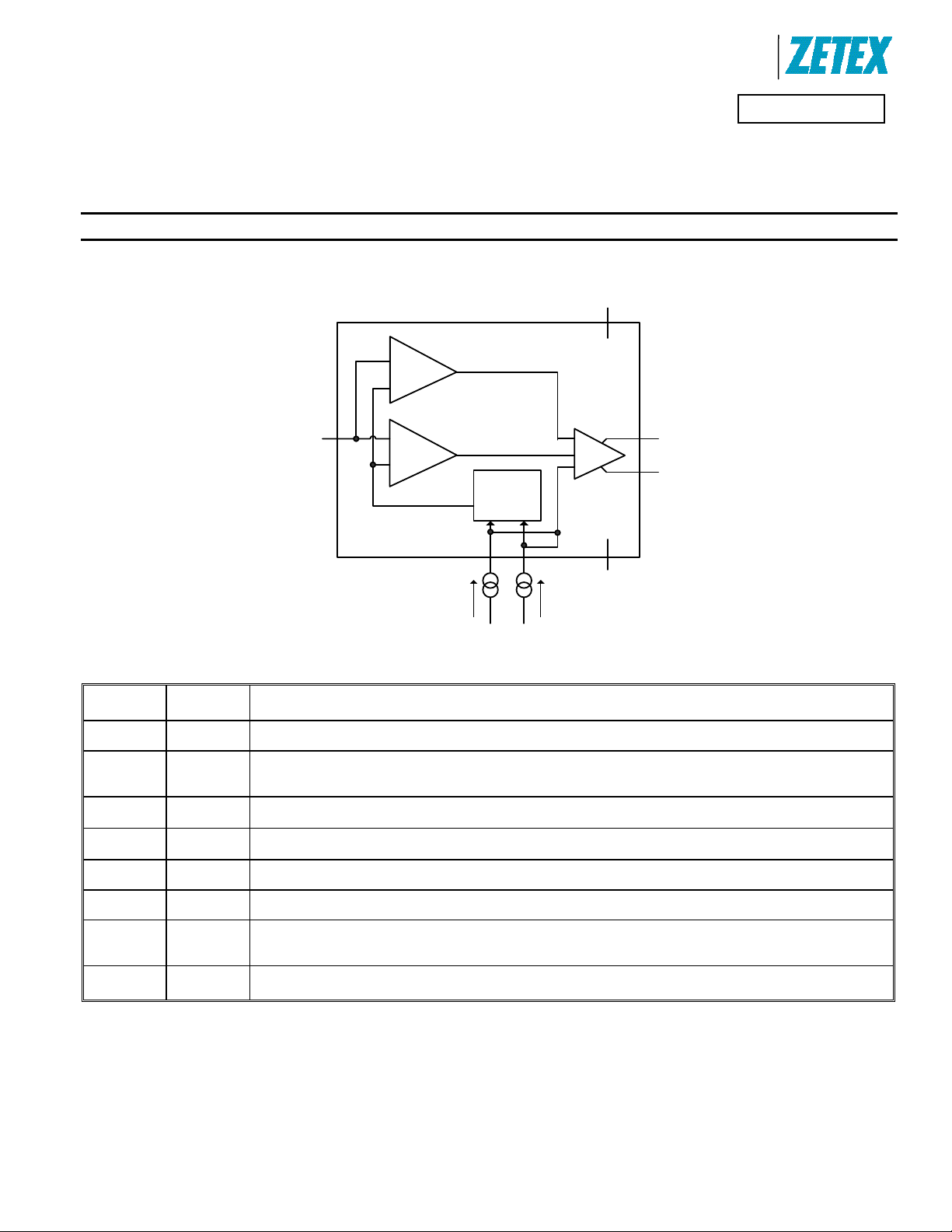
Schematic Symbol and Pin Out Details
+
Differential
amplifier
-
Product Line o
Diodes Incorporated
ZXGD3101N8
SYNCHRONOUS RECTIFIER CONTROLLER
Vcc
Gate drive
amplitude
control
DRAIN
+
High volt
-
comparator
Turn-on/off
control
Threshold
voltage
control
REF BIAS
GATEH
Driver
GATEL
GND
Pin No. Symbol Description and function
1 NC
2 REF
3 GATEL
4 GATEH
5
V
CC
6 GND
7 BIAS
8 DRAIN
Notes: 8. REF pin should be assumed to be at GND +0.7V.
9. BIAS pin should be assumed to be at GND +0.3V.
ZXGD3101N8
Document Number DS31945 Rev. 1 - 2
No connection
This pin can be connected to GND
Reference
This pin is connected to V
via resistor, R
CC
REF
. R
should be selected to source approximately 3mA into this pin.
REF
(Note 8)
Gate turn off
This pin sinks current, I
, from the synchronous MOSFET Gate.
SINK
Gate turn on
This pin sources current, I
Power Supply
This is the supply pin. It is recommended to decouple this point to ground closely with a ceramic capacitor.
, to the synchronous MOSFET Gate.
SOURCE
Ground
This is the ground reference point. Connect to the synchronous MOSFET Source terminal.
Bias
This pin is connected to V
via resistor, R
CC
BIAS
. R
should be selected to source 1.6 times I
BIAS
(Note 9)
Drain connection
This pin connects directly to the synchronous MOSFET Drain terminal.
4 of 14
www.diodes.com
into this pin.
REF
June 2010
© Diodes Incorporated

A
f
Product Line o
Diodes Incorporated
ZXGD3101N8
SYNCHRONOUS RECTIFIER CONTROLLER
Operation
Normal Operation
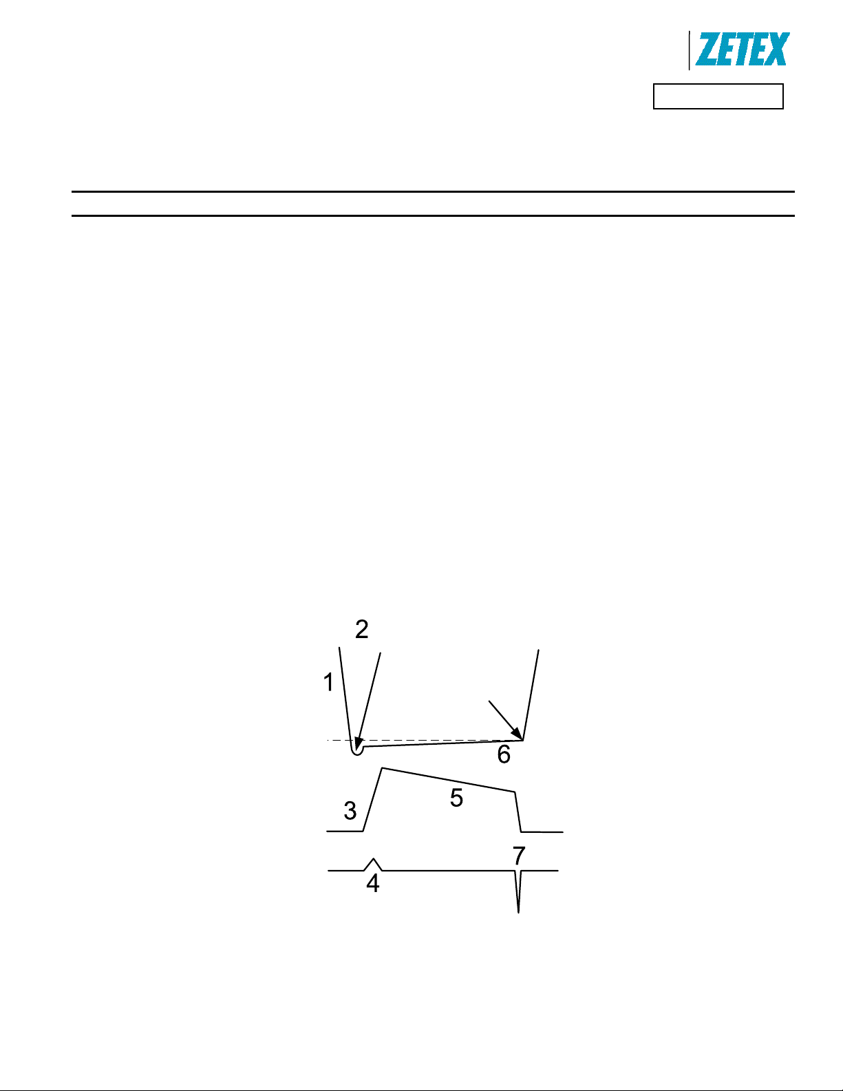
The operation of the device is described step-by-step with reference to the timing diagram below.
1. The detector monitors the MOSFET Drain-Source voltage.
2. When, due to transformer action, the MOSFET body diode is forced to conduct there is approximately -0.6V on the Drain pin.
3. The detector outputs a positive voltage with respect to ground, this voltage is then fed to the MOSFET driver stage and current is sourced out of
the GATEH pin.
4. The current out of the GATEH pin is sourced into the synchronous MOSFET Gate to turn the device on.
5. The GATEH output voltage is now proportional to the Drain-Source voltage drop across the MOSFET due to the current flowing through the
MOSFET.
6. MOSFET conduction continues until the drain current reaches zero.
7. At zero current the detector output voltage is zero and the synchronous MOSFET Gate voltage is pulled low by the GATEL, turning the device
off.
Body Diode
Conduction
Drain
current
zero
MOSFET
Gate Current
ZXGD3101N8
Document Number DS31945 Rev. 1 - 2
5 of 14
www.diodes.com
June 2010
© Diodes Incorporated
 Loading...