

Page 1
A
f
Product Line o
Description and Applications
The ZXGD3005E6 is a high-speed non-inverting single gate driver
capable of driving up to 10A into a MOSFET or IGBT gate capacitive
load from supply voltages up to 25V. With propagation delay times
down to <10ns and correspondingly rise/fall times of <20ns.
This gate driver ensures rapid switching of the MOSFET or IGBT to
minimize power losses and distortion in high current switching
applications. It is ideally suited to act as a voltage buffer between the
typically high output impedances of a controller IC and the effectively
low impedance on the gate of a power MOSFET or IGBT during
switching. Its low input voltage requirement and high current gain
allows high current driving from low voltage controller ICs.
The ZXGD3005E6 has separate source and sink outputs that enables
the turn-on and turn-off times of the MOSFET or IGBT to be
independently controlled. In addition, the wide supply voltage range
allows full enhancement of the MOSFET or IGBT to minimize on-state
losses and permits +15V to -5V gate drive voltage to prevent dV/dt
ADVANCE INFORMATION
induced false triggering of IGBTs. The ZXGD3005E6 has been
designed to be inherently rugged to latch-up and shoot-through
issues. The optimized pin-out SOT26 package eases board layout,
enabling reduced parasitic inductance of traces.
Power MOSFET and IGBT Gate Driving in:
• Synchronous switch-mode power supplies
• Power Factor Correction (PFC) in power supplies
• Secondary side synchronous rectification
• Plasma Display Panel power modules
• 1, 2 and 3-phase motor control circuits
• Audio switching amplifier power output stages
• Solar inverters
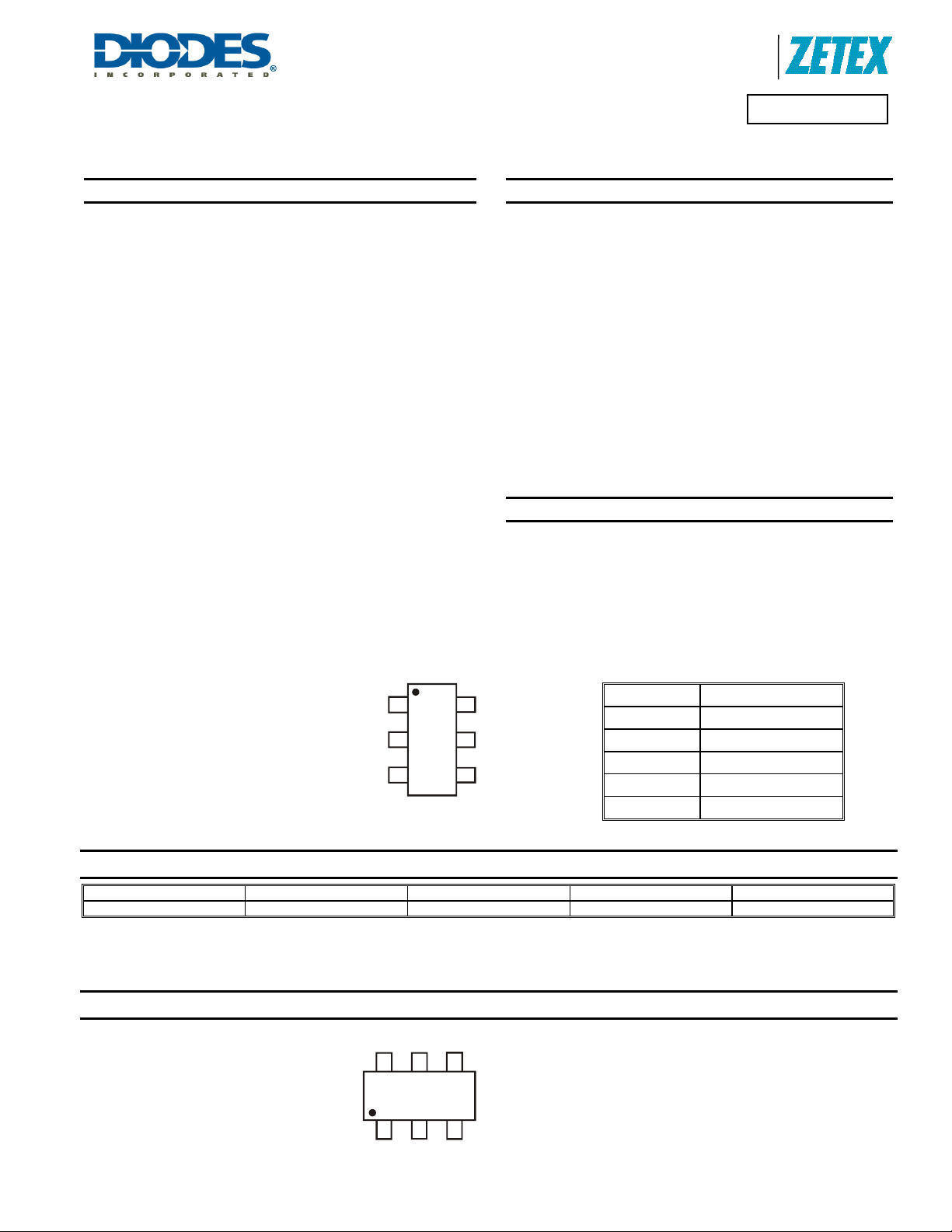
SOT26
1
Top View
V
CC
IN
V
EE
Top View
Pin-Out
Features and Benefits
• Emitter-follower configuration for ultra-fast switching
• <10ns propagation delay time
• <20ns rise/fall time
• Non-inverting voltage buffer stage
• Wide supply voltage up to 25V to minimize on-losses
• 10A peak current drive into capacitive loads
• Low input current of 1mA to deliver 4A output current
• Separate source and sink outputs for independent control of rise
and fall time
• Optimized pin-out to ease board layout and minimize parasitic
inductance of traces
• Rugged design that avoids latch-up or shoot-through issues
• Near - Zero quiescent supply current
• “Lead-Free”, RoHS Compliant (Note 1)
• “Green” Devices (Note 2)
• Qualified to AEC-Q101 Standards for High Reliability
Mechanical Data
• Case: SOT26
• Case material: Molded Plastic. “Green” Molding Compound.
• UL Flammability Rating 94V-0
• Moisture Sensitivity: Level 1 per J-STD-020
• Terminals: Matte Tin Finish
• Weight: 0.018 grams (approximate)
Source
Do Not Connect
Sink
Diodes Incorporated
ZXGD3005E6
25V 10A GATE DRIVER IN SOT26
Pin Name Pin Function
VCC
IN Driver input pin
VEE
SOURCE Source current output
SINK Sink current output
Supply voltage high
Supply voltage low
Ordering Information (Note 3)
Product Marking Reel size (inches) Tape width (mm) Quantity per reel
ZXGD3005E6TA 3005 7 8 3000
Notes: 1. No purposefully added lead
2. “Green” devices, Halogen and Antimony Free, Diodes Inc’s “Green” Policy can be found on our website at http://www.diodes.com
3. For packaging details, go to our website at http://www.diodes.com
Marking Information
3005
ZXGD3005E6
Document Number DS35095 Rev. 4 – 2
www.diodes.com
3005 = Product Type Marking Code
1 of 8
March 2011
© Diodes Incorporated
Page 2
A
f
(
)
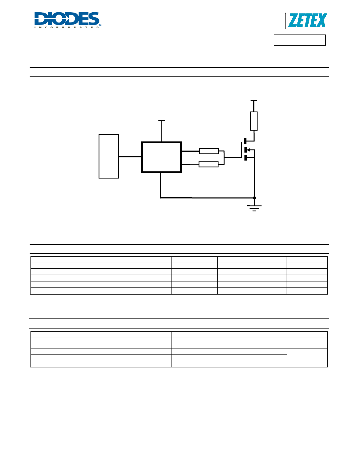
Typical Application Circuit
ADVANCE INFORMATION
Controller IC
IN
VCC
VCC
ZXGD3005
V
EE
SOURCE
SINK
R
SOURCE
R
SINK
Product Line o
Diodes Incorporated
V
ZXGD3005E6
S
Maximum Ratings @T
= 25°C unless otherwise specified
A
Characteristic Symbol Value Unit
Supply voltage, with respect to VEE
Input voltage, with respect to VEE
Output difference voltage (Source – Sink)
Peak output current
Input current
ΔV
V
CC
V
IN
source-sink
I
PK
I
IN
25 V
25 V
±7.5 V
±10 A
±100 mA
Thermal Characteristics @T
= 25°C unless otherwise specified
A
Characteristic Symbol Value Unit
Power Dissipation (Notes 4 & 5)
Linear derating factor
Thermal Resistance, Junction to Ambient (Notes 4 & 5)
Thermal Resistance, Junction to Lead (Note 6)
Operating and Storage Temperature Range
Notes: 4. For a device surface mounted on 25mm x 25mm x 0.6mm FR4 PCB with high coverage of single sided 1oz copper, in still air conditions; the device is
measured when operating in a steady-state condition. The heatsink is split in half with the pin 1 (V
5. For device with two active die running at equal power.
6. Thermal resistance from junction to solder-point at the end of each lead on pin 1 (V
P
R
R
T
J, TSTG
JA
JL
D
CC
CC
) and pin 3 (VEE).
1.1
8.8
113
105
-55 to +150
) and pin 3 (VEE) connected separately to each half.
W
mW/°C
°C/W
°C
ZXGD3005E6
Document Number DS35095 Rev. 4 – 2
2 of 8
www.diodes.com
March 2011
© Diodes Incorporated
Page 3
A
f
(
)
(
)
V
Product Line o
Diodes Incorporated
ZXGD3005E6
Electrical Characteristics @T
Characteristic Symbol Min Typ Max Unit Test Condition
Output voltage, high
Output voltage, low
Supply breakdown voltage
Quiescent supply current
Source current
Sink current
Source current
with varying input resistances
Sink current
with varying input resistances
ADVANCE INFORMATION
Switching times
with low load capacitance C
= 10nF
L
Switching times
with high load capacitance C
= 100nF
L
Switching times
with asymmetric source and sink resistors
Switching Test Circuit and Timing Diagram
= 25°C unless otherwise specified
A
V
OH
V
OL
BV
I
Q
I
source
I
sink
I
(source)
I
(sink)
t
d(rise)
t
t
d(fall)
tf
t
d(rise)
t
t
d(fall)
tf
CC
r
r
-
25 - 25 - -
- - 50
- - 50
- 4.0 -
- 3.8 -
-
-
-
-
VCC- 0.8
VEE+ 0.2 VEE+ 0.5 V
6.4
5.5
3.9
2.2
0.44
7.7
6.5
4.4
2.3
0.46
8
48
16
35
46
419
47
467
t
d(rise)
t
t
d(fall)
tf
r
24
133
16
37
-
- A
- A
- ns
- ns
ns
V
IN
V
IN
I
Q
V
I
Q
V
CC
nA
V
CC
VCC= 5V, IIN= 1mA, V
A
VCC= 5V, IIN=-1mA, V
R
IN
R
IN
R
IN
R
IN
R
IN
R
IN
R
IN
R
IN
R
IN
R
IN
V
CC
V
IN
R
IN
C
L
R
SOURCE
V
CC
V
IN
R
IN
C
L
R
SOURCE
V
CC
V
IN
R
IN
C
L
R
SOURCE
= VCC
= VEE
= 100μA, V
= 100μA, V
= 20V,V
= 20V,V
= 200
= 1k
= 10k
= 100k
= 1000k
= 200
= 1k
= 10k
= 100k
= 1000k
= 15V, V
= VCC
IN
= VEE = 0V
IN
= VCC
IN
= VEE = 0V
IN
OUT
OUT
V
= 15V, V
CC
V
= 15V
IN
C
= 100nF, RL = 0.18
L
R
SOURCE
= 15V, V
V
CC
= 15V
V
IN
C
= 100nF, RL = 0.18
L
R
SOURCE
= 0V
EE
= 0 to 15V
= 1k
= 10nF, RL = 0.18
= 0, R
= 15V, V
EE
SINK
= 0V
= 0
= 0 to 15V
= 1k
= 100nF, RL = 0.18
= 0, R
= 15V, V
EE
SINK
= -5V
= 0
= -5 to 15V
= 1k
= 10nF, RL = 0.18
=4.7, R
SINK
=0
= 0V
= 5V
EE
= 0, R
EE
= 0, R
= 0V
SINK
= 0V
SINK
= 0
= 0
R
SOURCE
R
SINK
90%
CL
L
V
IN
10%
t
t
d(rise)
90%
V
OUT
d(fall)
90%
V
OUT
R
V
50
VIN
50
RIN
IN
CC
VCC
ZXGD3005
V
EE
SOURCE
SINK
10%
10%
ZXGD3005E6
Document Number DS35095 Rev. 4 – 2
www.diodes.com
3 of 8
tr
t
f
March 2011
© Diodes Incorporated
Page 4

A
f
Typical Switching Characteristics @T
= 25°C unless otherwise specified
A
Product Line o
Diodes Incorporated
ZXGD3005E6
15
10
V
OUT
5
Voltage (V )
V
IN
VIN = 0 to 15V
VCC= 15V
VEE= 0V
RIN = 1kΩ
CL = 10nF
RL = 0.18Ω
R
= 0Ω
SOURCE
R
= 0Ω
SINK
0
15
10
V
OUT
5
Voltage (V )
V
IN
0
VIN = 0 to 15V
VCC= 15V
VEE= 0V
RIN = 1kΩ
CL = 100nF
RL = 0.18Ω
R
= 0Ω
SOUR CE
R
= 0Ω
SINK
ADVANCE INFORMATION
0 100 200 300 400 500 600 700 800
Time (ns)
Switch ing Speed
Low Load Capacitan ce CL = 10nF
15
10
V
OUT
5
0
Voltage (V )
V
IN
-5
0 100 200 300 400 500 600 700 800
Time (ns)
Switching Speed
Asymmetric Source and Sink Resistors
VIN = -5 to 15V
VCC= 15V
VEE= -5V
RIN = 1kΩ
CL = 10nF
RL = 0.18Ω
R
SOURCE
R
SINK
= 4.7Ω
= 0Ω
Supply Current (A)
0.0 0.5 1.0 1.5 2.0 2.5 3.0 3.5
Time (
μs)
Switch ing S p eed
High Loa d Ca pa citance CL = 100nF
10
0.1
0.01
VIN = 0 to 15V
VCC= 15V
1
VEE= 0V
Square Wave
CL= 1μF
CL= 100nF
1E-3
1E-4
10 100 1k 10k 100k 1M
Frequency (Hz)
Supply Current
CL= 1nF
CL= 10nF
ZXGD3005E6
Document Number DS35095 Rev. 4 – 2
www.diodes.com
4 of 8
March 2011
© Diodes Incorporated
Page 5

A
f
Typical Switching Characteristics @T
= 25°C unless otherwise specified
A
Product Line o
Diodes Incorporated
ZXGD3005E6
10
1
VIN = 15V
0.1
VCC= 15V
VEE= 0V
RL = 0.18Ω
0.01
ADVANCE INFORMATION
Peak Source Current (A)
1k 10k 100k 1M 10M
CL=1uF
CL=100nF
CL=10nF
CL=1nF
RIN Inp ut Resistance (Ω)
Source Current vs. Input Resistance
1000
(ns)
t
RIN=1MΩ
RIN=100kΩ
100
VIN = 15V
d(rise)
10
RIN=200Ω
1
1 10 100 1k
RIN=1kΩ
RIN=10kΩ
VIN = 15V
VCC= 15V
VCC= 15V
VEE= 0V
VEE= 0V
RL = 0.18Ω
RL = 0.18Ω
CL Load Capacitance (nF)
Turn-O n Delay Time
10
1
VIN = 15V
0.1
VCC= 15V
VEE= 0V
Peak Sink Current (A)
RL = 0.18Ω
0.01
1k 10k 100k 1M 10M
RIN Input Resistance (Ω)
Sink Current vs. Input Resistance
RIN=1MΩ
1000
RIN=100kΩ
100
(ns)
d(fall)
t
10
RIN=200Ω
1
1 10 100 1k
RIN=1kΩ
RIN=10kΩ
CL Load Capacitance (nF)
Turn-O ff D e lay Time
CL=1uF
CL=100nF
CL=10nF
CL=1nF
VIN = 15V
VCC= 15V
VEE= 0V
RL = 0.18Ω
10000
1000
(ns)
t
RIN=1MΩ
RIN=100kΩ
RIN=10kΩ
r
100
RIN=1kΩ
10
1 10 100 1k
RIN=200Ω
VIN = 15V
VCC= 15V
VEE= 0V
RL = 0.18Ω
10000
(ns)
f
t
CL Load Capacitance (nF)
Turn-O n Rise Time
ZXGD3005E6
Document Number DS35095 Rev. 4 – 2
5 of 8
www.diodes.com
RIN=1MΩ
RIN=100kΩ
1000
RIN=10kΩ
100
RIN=1kΩ
10
1 10 100 1k
RIN=200Ω
CL Load Capacitance (nF)
Turn-O ff F all Time
VIN = 15V
VCC= 15V
VEE= 0V
RL = 0.18Ω
© Diodes Incorporated
March 2011
Page 6

A
f
Application Notes
Independent control of rise and fall time
An application may require the turn-on (t
to be independently controlled, which can be achieved by setting
different R
and R
SINK
the SOURCE and SINK pins during the switching transition. If the
potential difference across the SOURCE and SINK pins is greater
than 7.5V, then it could damage the ZXGD3005.
In this circuit example of driving an IGBT, a blocking diode is
added in series with R
current being induced into the SINK pin.
and R
SOURCE
resistors, then a potential difference will occur between
values. With asymmetric R
SINK
to protect against excess reverse
SINK
) and turn-off (t
on
) time
off
SOURCE
Product Line o
Diodes Incorporated
ZXGD3005E6
ADVANCE INFORMATION
Circuit example of driving a MOSFET
Application example of gate driving a MOSFET from 0 to 15V with
R
SOURCE
= R
SINK
= 0
Switching Time Characteristic
15
10
V
OUT
5
Voltage (V)
0
V
IN
VIN = 0 to 15V
VCC= 15V
VEE= 0V
RIN = 1kΩ
CL = 10nF
RL = 0.18Ω
R
R
SOURCE
SINK
= 0Ω
= 0Ω
Circuit example of driving an IGBT
Application example of gate driving an IGBT with independent t
t
using asymmetric R
off
driven from -5 to +15V to prevent dV/dt induced false triggering.
SOURCE
and R
In addition, the gate is
SINK
Switching Time Characteristic
15
10
V
5
0
Voltage (V)
-5
OUT
V
IN
VIN = -5 to 15V
VCC= 15V
VEE= -5V
RIN = 1kΩ
CL = 10nF
RL = 0.18Ω
R
= 4.7Ω
SOURCE
R
= 0Ω
SINK
on
and
0 100 200 300 400 500 600 700 800
Time (ns)
Symmetric So urce an d Sink Resistor s
0 100 200 300 400 500 600 700 800
Time (ns)
Asy mme tr ic Sour ce and Sink Re sis to r s
ZXGD3005E6
Document Number DS35095 Rev. 4 – 2
6 of 8
www.diodes.com
March 2011
© Diodes Incorporated
Page 7

A
f
Package Outline Dimensions
ADVANCE INFORMATION
K
J
Suggested Pad Layout
Product Line o
Diodes Incorporated
ZXGD3005E6
A
B C
H
M
D
L
Dim Min Max Typ
SOT26
A 0.35 0.50 0.38
B 1.50 1.70 1.60
C 2.70 3.00 2.80
D
⎯ ⎯
H 2.90 3.10 3.00
J 0.013 0.10 0.05
K 1.00 1.30 1.10
L 0.35 0.55 0.40
M 0.10 0.20 0.15
0° 8°
α
All Dimensions in mm
0.95
⎯
C2
C2
Dimensions Value (in mm)
Z 3.20
G
Z
Y
X
C1
G 1.60
X 0.55
Y 0.80
C1 2.40
C2 0.95
ZXGD3005E6
Document Number DS35095 Rev. 4 – 2
7 of 8
www.diodes.com
March 2011
© Diodes Incorporated
Page 8

A
f
Product Line o
Diodes Incorporated
ZXGD3005E6
DIODES INCORPORATED MAKES NO WARRANTY OF ANY KIND, EXPRESS OR IMPLIED, WITH REGARDS TO THIS DOCUMENT,
INCLUDING, BUT NOT LIMITED TO, THE IMPLIED WARRANTIES OF MERCHANTABILITY AND FITNESS FOR A PARTICULAR PURPOSE
(AND THEIR EQUIVALENTS UNDER THE LAWS OF ANY JURISDICTION).
Diodes Incorporated and its subsidiaries reserve the right to make modifications, enhancements, improvements, corrections or other changes
without further notice to this document and any product described herein. Diodes Incorporated does not assume any liability arising out of the
application or use of this document or any product described herein; neither does Diodes Incorporated convey any license under its patent or
trademark rights, nor the rights of others. Any Customer or user of this document o r products described herein in such applica tions shall assume
all risks of such use and will agree to hold Diodes Incorporated and all the companies whose products are represented on Diodes Incorporated
website, harmless against all damages.
Diodes Incorporated does not warrant or accept any liability whatsoever in respect of any products purchased through unauthorized sales channel.
Should Customers purchase or use Diodes Incorporated products for any unintended or unauthorize d application, Customers shall indemnify and
hold Diodes Incorporated and its representatives harmless against all claims, damages, expenses, and attorney fees arising out of, directly or
indirectly, any claim of personal injury or death associated with such unintended or unauthorized application.
Products described herein may be covered by one or more United States, international or foreign patents pending. Product names and markings
ADVANCE INFORMATION
noted herein may also be covered by one or more United States, international or foreign trademarks.
Diodes Incorporated products are specifically not authorized for use as critical components in life support devices or systems without the express
written approval of the Chief Executive Officer of Diodes Incorporated. As used herein:
A. Life support devices or systems are devices or systems which:
1. are intended to implant into the body, or
labeling can be reasonably expected to result in significant injury to the user.
B. A critical component is any component in a life support device or system whose failure to perform can be reasonably expected to cause the
failure of the life support device or to affect its safety or effectiveness.
Customers represent that they have all necessary expertise in the safety and regulatory ramifications of their life support devices or systems, and
acknowledge and agree that they are solely responsible for all legal, regulatory and safety-related requirements concerning their products and any
use of Diodes Incorporated products in such safety-critical, life support devices or systems, notwithstanding any devices- or systems-related
information or support that may be provided by Diodes Incorporated. Further, Customers must fully indemnify Diodes Incorporated and its
representatives against any damages arising out of the use of Diodes Incorporated products in such safety-critical, life support devices or systems.
Copyright © 2011, Diodes Incorporated
www.diodes.com
2. support or sustain life and whose failure to perform when properly used in accordance with instructions for use provided in the
IMPORTANT NOTICE
LIFE SUPPORT
ZXGD3005E6
Document Number DS35095 Rev. 4 – 2
8 of 8
www.diodes.com
March 2011
© Diodes Incorporated
 Loading...