Diodes ZXCT1107, ZXCT1109, ZXCT1110 User Manual
A
Product Line o
f
Diodes Incorporated
NEW PRODUCT
LOW POWER HIGH-SIDE CURRENT MONITORS
Description
The ZXCT1107/09/10 are high side unipolar current sen se
monitors. These devices eliminate the need to disrupt the
ground plane when sensing a load current.
The wide common-mode input voltage range and low
quiescent current coupled with SOT23 packages make
them suitable for a range of applications; including
adapters, automotive and systems operating from industrial
24V rails.
The device is line powered and as such doesn’t need a
separate supply rail.
Quiescent current is only 3µA thereby minimising current
sensing error. One external gain setting resistor increases
versatility by permitting wide gain ranges.
Features
• Wide supply and common-mode voltage range:
2.5V to 36V
• SOT23 packages
o 3-pin ZXCT1107/09
o 5-pin ZXCT1110
• Low quiescent current (3µA).
• Extended industrial temperature range -40 to 125°C
• AEC-Q100 Grade1 Automotive qualified variants
Applications
• Automotive current measurement
• Industrial applications current measurement
• Battery management
• Over current monitor
• Power Management
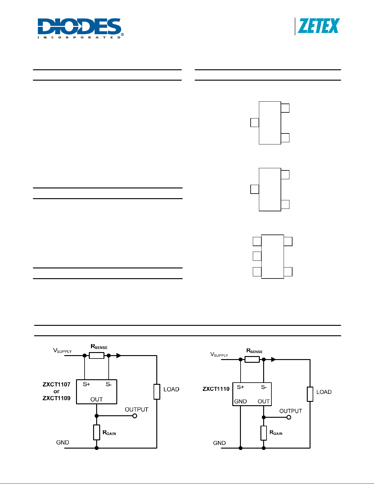
Pin Assignments
OUT 1
OUT 1
OUT 1
OUT 1
NC 1
NC 1
GND 2
GND 2
OUT 3
OUT 3
ZXCT1107/1109/1110
ZXCT1107
Top View
2 S-
2 S-
3 S+
ZXCT1109
Top View
ZXCT1110
Top View
3 S+
2 S+
2 S+
3 S-
3 S-
4 S+
4 S+
5 S-
5 S-
Typical Application Circuit
ZXCT1107/1109/1110
Document number: DS35033 Rev. 3 - 2
1 of 16
www.diodes.com
JULY 2011
© Diodes Incorporated
A
Product Line o
f
Diodes Incorporated
NEW PRODUCT
ZXCT1107/1109/1110
LOW POWER HIGH-SIDE CURRENT MONITORS
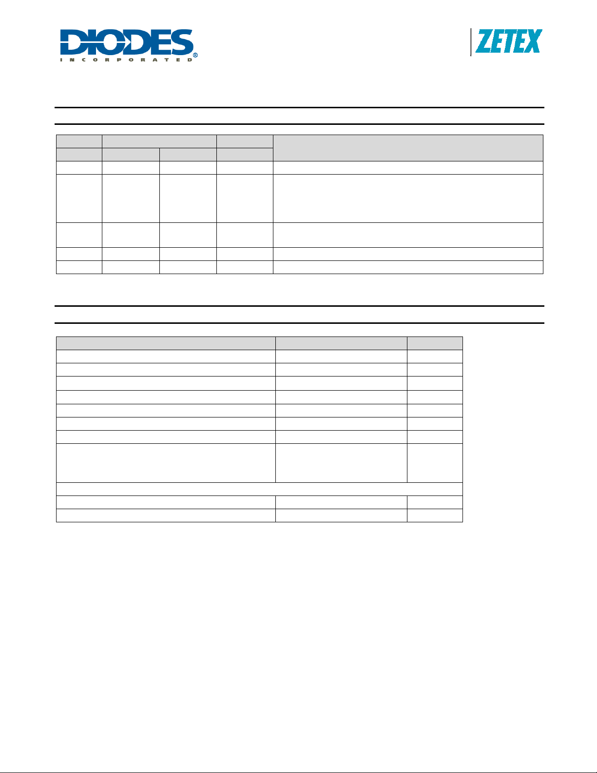
Pin Descriptions
Package SOT23 SOT25
Name ZXCT1107 ZXCT1109 ZXCT1110
OUT 11 1
1
3 Output pin. Current output.
Description
This is the positive input of the current monitor and has a wide
S+ 3 2 4
common-mode input range. This also acts as the analog supply and
provides power to internal circuitry. The current through this pin
varies with differential sense voltage.
S- 2 3 5
This is the negative input of the current monitor and has a wide
common-mode input range.
GND - - 2 Ground pin and substrate connection.
NC - - 1 No connection
Notes. 1. For the ZXCT1107 and ZXCT1109 pin 1 (OUT) acts as both the output pin and substrate connection. This means that for the
ZXCT1107 and ZXCT1109 the minimum rail voltage that can be used is 2.5V + V
(see applications section for more details).
OUT
Absolute Maximum Ratings
Description Rating Unit
Voltage on S- and S+ relative to OUT (ZXCT1107/9) -0.3 to 40 V
Voltage on S- and S+ relative to GND (ZXCT1110) -0.3 to 40 V
Voltage on OUT to GND (ZXCT1110)
Differential Sense Voltage, V
SENSE
2,3
-0.3 to V
-0.3 to 0.8 V
Current into S+ and S-3 ±8.5 mA
Storage Temperature -55 to 150 °C
Maximum Junction Temperature 150 °C
Package Power Dissipation (TA = 25°C)
SOT23
SOT25
300 (De-rate to Zero at 150°C)
300 (De-rate to Zero at 150°C)
ESD Ratings
Human Body Model 1000 V
Machine Model 150 V
S+
V
mW
Operation above the absolute maximum rating may cause device failure. Operation at the absolute maximum ratings,
for extended periods, may reduce device reliability.
Notes: 2. V
3. The differential input voltage limit, V
ZXCT1107/1109/1110
Document number: DS35033 Rev. 3 - 2
SENSE
= VS+ - VS-
- V
, may be exceeded provided that the input current limit into S+ or S- is not exceeded.
S+
S-
2 of 16
www.diodes.com
JULY 2011
© Diodes Incorporated
A
Product Line o
f
Diodes Incorporated
ZXCT1107/1109/1110
LOW POWER HIGH-SIDE CURRENT MONITORS
Recommended Operating Conditions
Symbol Parameter Min Max Unit
ZXCT1110 2.5 36
4
:
SENSE
100mV)
SENSE
ZXCT1107/9
V
OUT(MAX)
+ 2.5
0 0.5 V
ZXCT1110 0
ZXCT1107/9 0
-40 125 °C
(see applications section for more details).
OUT
5
= 100mV, R
= 0 unless otherwise stated)
GAIN
V
V
S+
36
- 1
S-
- 2.5
V
V
NEW PRODUCT
VS+
V
SENSE
V
Output voltage range (0 V
OUT
TA
Notes. 4. For the ZXCT1107 and ZXCT1109 pin 1 (OUT) acts as both the output pin and substrate connection. This means that for the
ZXCT1107 and ZXCT1109 the minimum rail voltage that can be used is 2.5V + V
Common-mode input range
Differential Sense Input voltage range (VS+-VS-)
Ambient temperature range
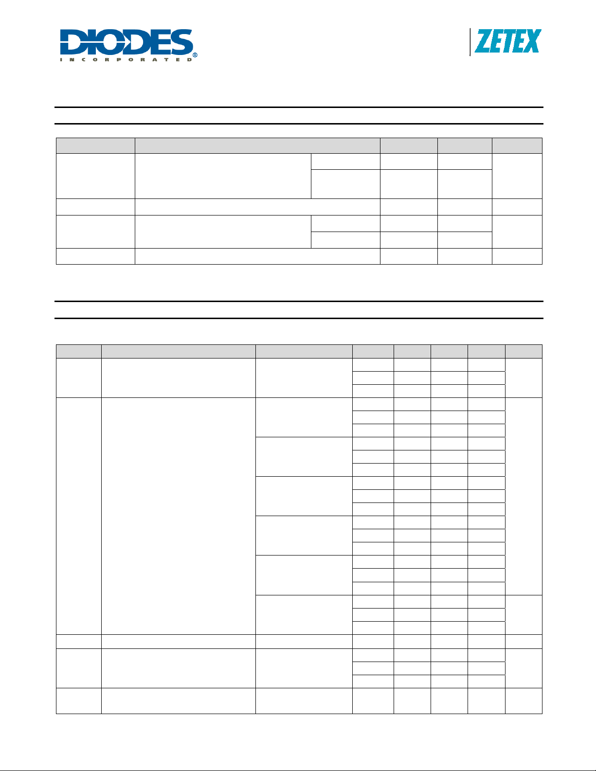
Electrical Characteristics (T
= 25°C, VS+ = 20V, V
A
ZXCT1107, ZXCT1109
Symbol Parameter Conditions
IS-
I
OUT
I
OUT -TC
S- input current
Output current
Output current temperature coefficient full range 370 ppm/ºC
6
CMSR Common-Mode Sense rejection
BW -3dB Small Signal Bandwidth
5
V
V
V
V
V
V
V
V
V
R
= 0V
SENSE
5
= 0mV
SENSE
5
= 10mV
SENSE
5
= 30mV
SENSE
5
= 100mV
SENSE
5
= 200mV
SENSE
5
= 500mV
SENSE
= 2.5V to 36V
S+
SENSE5 (AC)
= 2.5k
GAIN
= 10mV
TA
25°C 19 100
-40°C 16
125°C 35
25°C 1 3 10
-40°C 2.2
125°C 5.5
25°C 37 45 54
-40°C 42
125°C 49
25°C 115 124 134
-40°C 119
125°C 129
25°C 394 408 422
-40°C 396
125°C 420
25°C 787 810 832
-40°C 785
125°C 832
25°C 1.965 2.015 2.064
-40°C 1.965
125°C 2.065
25°C 0.1 0.4
-40°C 0.13
125°C 0.05
PP
25°C 0.65 MHz
Min Typ Max Units
nA
µA
mA
µA/V
ZXCT1107/1109/1110
Document number: DS35033 Rev. 3 - 2
3 of 16
www.diodes.com
JULY 2011
© Diodes Incorporated
A
Product Line o
f
Diodes Incorporated
NEW PRODUCT
LOW POWER HIGH-SIDE CURRENT MONITORS
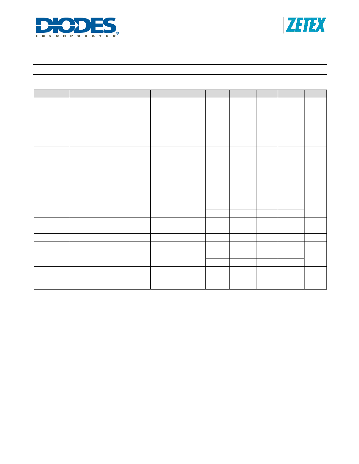
Electrical Characteristics (T
ZXCT1110
Symbol Parameter Conditions
IQ
IS-
CMSR Common-Mode Sense rejection
IOO
GT
GE Transconductance error
I
OUT GT-TC
V
OUTH
BW -3dB Small Signal Bandwidth
GND pin current
S- input current
Output Offset current
Transconductance
Transconductance temp.co 25°C 265 ppm/ºC
Output relative to VS-
= 25°C, VS+ = 20V, V
A
V
SENSE
V
S+
6,7
V
SENSE
V
SENSE
150mV
V
SENSE
150mV
V
SENSE5 (AC)
10mV
2.5k
5
= 2.5V to 36V
5
5
5
PP, RGAIN
5
SENSE
= 0V
= 10mV
= 10mV to
= 10mV to
=
=
ZXCT1107/1109/1110
= 100mV, R
TA
25°C 3 5
-40°C 2.2
125°C 5.8
25°C 19 100
-40°C 16
125°C 35
25°C 0.1 0.4
-40°C 0.13
125°C 0.05
25°C 0 ±4
-40°C -1.8
125°C +2.5
25°C 3.928 4 4.072
-40°C 3.9
125°C 4.08
25°C -1.8 1.8 %
25°C -1 -0.78
-40°C -0.88
125°C -0.63
25°C 0.65 MHz
= 0 unless otherwise stated) (cont.)
GAIN
Min Typ Max Units
µA
nA
µA/V
µA
mA/V
V
Notes. 5. V
6. Output current characteristic measured with low impedance ammeter connected to GND
7. Defined as difference between actual output current and 40µA; measured at V
currents of the device.
8. For V
SENSE
= “V
SENSE
” – “V
SENSE+
> 10mV, the internal voltage-current converter is fully linear. This enables a true offset to be defined and used.
SENSE
“
-
=10mV. This will include an error due to bias
SENSE
ZXCT1107/1109/1110
Document number: DS35033 Rev. 3 - 2
4 of 16
www.diodes.com
JULY 2011
© Diodes Incorporated
A
Product Line o
f
A
A
Diodes Incorporated
NEW PRODUCT
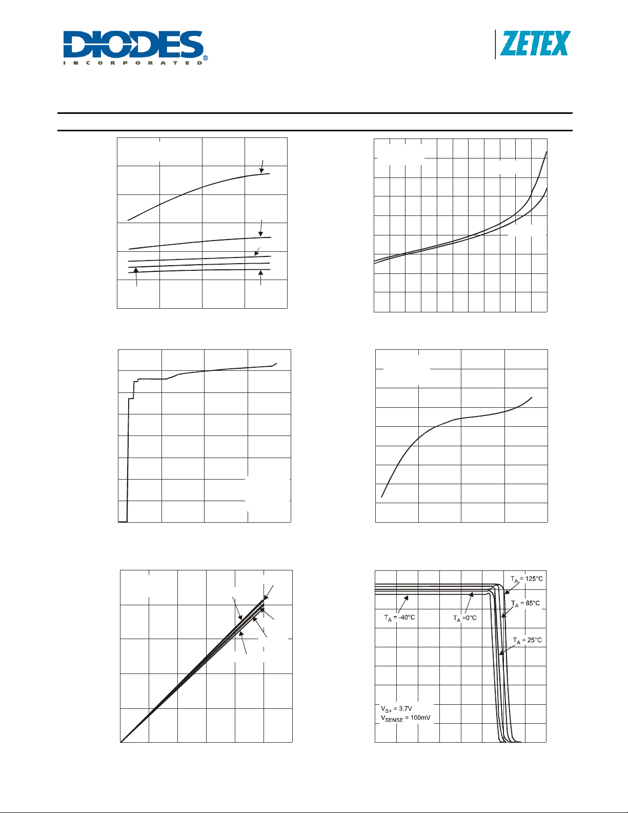
Typical Characteristics
12
V = 0V
OUT
V = 0V
SENSE
10
8
)
6
S+
I (µ
4
2
T = 0°C
A
0
010203040
4.0
3.5
3.0
2.5
2.0
S+
I (µA)
1.5
1.0
0.5
0.0
010203040
V (V)
Input Current vs. V
V (V)
I Current vs. V
S+ S+
ZXCT1107/1109/1110
LOW POWER HIGH-SIDE CURRENT MONITORS
9.0
V = 0V
T = 125°C
A
T = 85°C
A
T = 25°C
A
T = -40°C
A
S+
S+
I (µA)
S+
I (nA)
T = 25°C
A
V = 0V
OUT
V = 0V
SENSE
S+
SENSE
8.0
V = 0V
OUT
7.0
V = 20V
S+
6.0
5.0
V = 3.7V
4.0
S+
3.0
2.0
1.0
0.0
-40 -25 -10 5 20 35 50 65 80 95 110 125
TEMPERATURE (°C)
Input Current vs. A m bi ent Temperature
1.8
T = 25°C
A
V = 0V
1.6
OUT
V = 0V
SENSE
1.4
1.2
1.0
S-
0.8
0.6
0.4
0.2
0.0
010203040
V (V)
S+
I Current vs. V
S- S+
2500
2000
1500
)
OUT
I (µ
1000
V = 20V
S+
V = 0V
OUT
T = 125°C
A
T = -40°C
A
T = 85°C
A
T =25°C
A
T = 0°C
A
450
400
350
300
250
200
150
OUTPUT CURRENT (µA)
500
100
50
0
0 100 200 300 400 500 600
ZXCT1107/1109/1110
Document number: DS35033 Rev. 3 - 2
V (mV)
SENSE
Output Current vs. V
SENSE
5 of 16
www.diodes.com
0
0.0 0.5 1.0 1.5 2.0 2.5 3.0 3.5 4.0
OUTPUT VOLTAGE (V )
Output Cu r r e nt vs. Output Voltage
JULY 2011
© Diodes Incorporated
 Loading...