Diodes ZXCT1082, ZXCT1083, ZXCT1084, ZXCT1085, ZXCT1086 User Manual
...
A
Product Line o
f
Diodes Incorporated
ZXCT1082/83/84/85/86/87
PRECISION HIGH VOLTAGE HIGH-SIDE CURRENT MONITORS
Description
The ZXCT1082 and ZXCT1083 are high side unipolar
current sense monitors. These devices eliminate the need to
disrupt the ground plane when sensing a load current.
The ZXCT1082/1084/1086 have 60V maximum operating
voltage and ZXCT1083/1085/1087 have 40V maximum
operating voltage.
The wide common-mode input voltage range and low
quiescent currents coupled with SOT25 packages make
them suitable for a range of applications; including
automotive and systems operating from industrial 24-28V
rails.
Their quiescent current is only 0.6µA thereby minimizing
current sensing error.
The ZXCT1082 and ZXCT1083 use three external
transconductance/gain setting resistors which increase
versatility by permitting wide gain ranges and optimization of
bandwidths.
The ZXCT1084/5/6/7 are fixed gain voltage output
counterparts of the ZXCT1082/3.
Features
• Wide supply and common-mode voltage range
o 2.7V to 60V ZXCT1082/84/86
o 2.7V to 40V ZXCT1083/85/87
• Independent supply and input common-mode voltage
• Low quiescent current (0.6µA).
• AEC-Q100 Grade 1 qualified
• Extended industrial temperate range -40 to 125°C
• Package SOT25
Applications
• Automotive current measurement
• Industrial applications current measurement
• Battery management
• Over current monitor
• Power Management
• Current sources
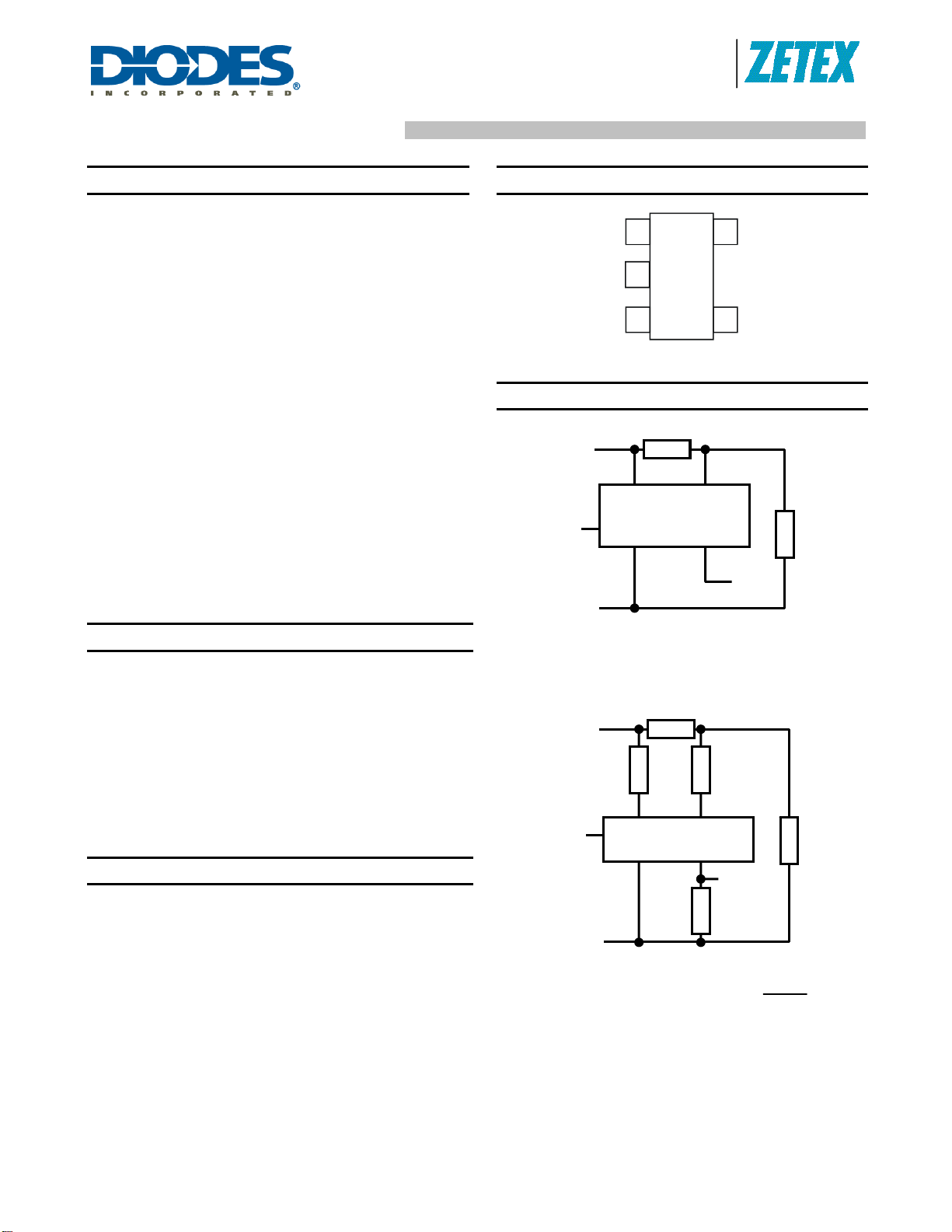
Pin Assignments
OUT
GND
1
2
5
S+
34
Typical Application Circuits
R
SENSE
R
SENSE
R
GT
OUT
OUT
OUT
= V
S-
OUT
= 25 x V
= 50 x V
R
GT
S-
OUT
R
G
SENSE
V
SUPPLY
S+
ZXCT1084/1085
V
ZXCT1086/1087
CC
GND
ZXCT1084/85: V
ZXCT1086/87: V
V
SUPPLY
S+
V
ZXCT1082/1083
CC
GND
ZXCT1082/83: V
V
S-
CC
* R
R
V
LOAD
Load
SENSE
SENSE
V
Load
G
GT
LOAD
ZXCT1082/83/84/85/86/87
Document number: DS32162 Rev. 2 - 2
1 of 13
www.diodes.com
June 2011
© Diodes Incorporated

A
f
Pin Description
Product Line o
Diodes Incorporated
ZXCT1082/83/84/85/86/87
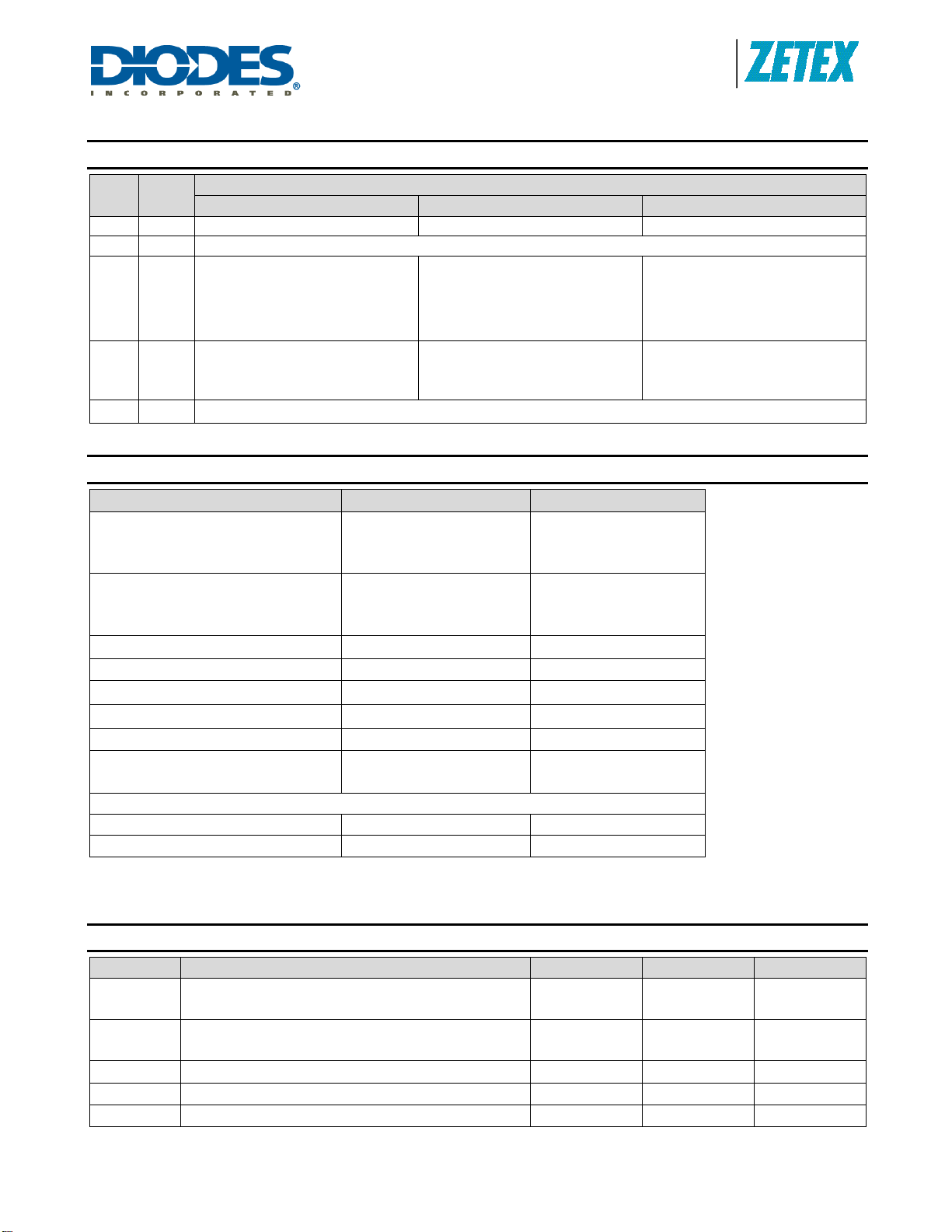
PIN Name
Common ZXCT1082/3 ZXCT1084/5/6/7
Description
1 OUT Output pin. Current output. Voltage output
2 GND Ground pin.
3 S+
4 S-
5
V
This is the positive input of the
current monitor. It has a wide
common-mode input range. The
current through this pin varies with
differential sense voltage.
This is the negative input of the
current monitor. It has a wide
common-mode input range.
This is the analogue supply and provides power to internal circuitry.
CC
An external resistor, R
be connected from S+ to the input
side (V
SUPPLY
) of the sense
resistor
An external resistor, R
be connected from S- to the load
side (V
) of the sense resistor.
LOAD
, should
GT
, should
GT
Should be directly connected to
the input side (V
sense resistor.
Should be directly connected to
the load side (V
resistor.
Absolute Maximum Ratings
Parameter Rating Unit
Voltage on S- and S+
ZXCT1082, ZXCT1084, ZXCT1086
ZXCT1083, ZXCT1085, ZXCT1087
Voltage on V
CC
ZXCT1082, ZXCT1084, ZXCT1086
ZXCT1083, ZXCT1085, ZXCT1087
Voltage on OUT
Differential Input Voltage, VS+ - VSInput current into S+ or S-
(†)
Storage Temperature -55 to 150 °C
Maximum Junction Temperature 150 °C
Package Power Dissipation
300 at T
(De-rate to zero at 150°C)
ESD Rating
Human Body Model 2 kV
Machine Model 200 V
Operation above the absolute maximum rating may cause device failure. Operation at the absolute maximum ratings, for
extended periods, may reduce device reliability.
(†)
The differential input voltage limit, V
- VS- may be exceeded provided that the input current limit into S+ or S- is not exceeded
S+
-0.3 to 65
V
-0.3 to 45
-0.3 to 65
V
-0.3 to 45
-0.3 to V
S-
V
±800 mV
±12 mA
= 25°C
A
mW
SUPPLY
) of the sense
LOAD
) of the
Recommended Operating Conditions
Symbol Parameter Min Max Units
VIN
VCC
V
SENSE
V
OUT
TA
ZXCT1082/83/84/85/86/87
Document number: DS32162 Rev. 2 - 2
ZXCT1083/1085/1087 Common-Mode Input Range
ZXCT1082/1084/1086 Common-Mode Input Range
ZXCT1083/1085/1087 Supply Voltage Range
ZXCT1082/1084/1086 Supply Voltage Range
Differential Sense Input Voltage Range 0 0.5 V
Output Voltage Range 0
Ambient Temperature Range -40 125 °C
2 of 13
www.diodes.com
2.7
2.7
2.7
2.7
40
60
40
60
VS- -1
V
V
V
June 2011
© Diodes Incorporated

A
Product Line o
f
Diodes Incorporated
ZXCT1082/83/84/85/86/87
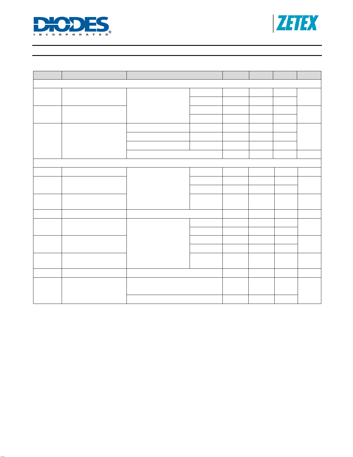
Electrical Characteristics
Test Conditions TA = 25°C, VS+ = 12V, VCC = 5 V, V
(FT = -40°C to +125°C)
Symbol Parameter Conditions Min. Typ. Max. Units
Input
IS+
S+ input current
V
IS-
S- input current
V
VIO
Input Offset Voltage
(Note 2)
ZXCT1082/3/4/5
ZXCT1086/87
Temperature co-efficient ±4 µV/K
Output
G
G
Z
GT
T-ERR
T-TC
OUT
GV
Transconductance
Transconductance error
(Note 4)
Transconductance
temperature co-efficient
Output impedance ZXCT1082/3 1¦¦5 GΩ¦¦pF
ZXCT1082/3
V
(Note 1, 3)
Gain
ZXCT1084/5/6/7
G
V-ERR
Gain error (Note 4)
V
(Note 1)
G
V-TC
Z
OUT
V
OUTH
Notes: 1. For the ZXCT1082/83 V
For the ZXCT1083/84/85/86 V
Voltage gain temperature
co-efficient
Output impedance ZXCT1084/5/6/7 125 kΩ
Output relative to common
mode, V
2. V
is extrapolated from measurements for the gain-error test.
IO
3. For V
SENSE
4. Gain or transconductance error is calculated by applying two values of V
S-
SENSE
> 10mV, the internal voltage-current converter is fully linear. This enables a true offset to be defined and used.
ZXCT1082/3
ZXCT1084/5/6/7
= “V
SUPPLY
= “VS+” – “VS-“
SENSE
1
= 100mV, ZXCT1082/3 RGT = 5kΩ, RG = 125kΩ; unless otherwise stated.
SENSE
= 0mV (Note 1)
SENSE
= 0mV
SENSE
= 10mV to 150mV
SENSE
= 10mV to 150mV
SENSE
” – “V
LOAD
“ where V
1.7
TA = FT
5
1.7
TA = FT
5
±0.2 ±1
T
T
= FT
A
= FT
A
±2.5
±3
200 µA/V
-1 +1
TA = FT
= FT
T
A
-2 +2
10 nA/K
1084/5 25
1086/7 50
-1 +1
TA = FT
= FT
T
A
is the load voltage or the lower potential side of the sense resistor.
LOAD
and calculating the error of the slope vs. the ideal.
SENSE
-2 +2
100 ppm/K
V
LOAD
- 1
V
LOAD
V
S-
- 1 V
- 0.8
- 0.8
S-
µA
µA
mV
%
V/V
%
V
ZXCT1082/83/84/85/86/87
Document number: DS32162 Rev. 2 - 2
3 of 13
www.diodes.com
June 2011
© Diodes Incorporated

A
Product Line o
f
Diodes Incorporated
ZXCT1082/83/84/85/86/87
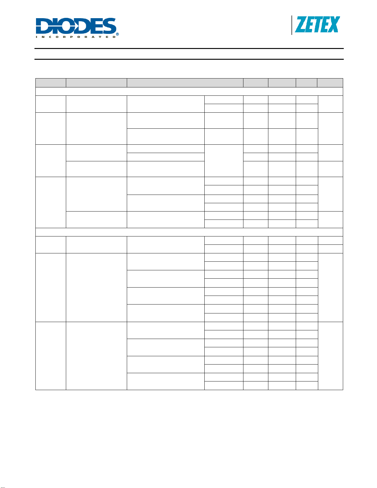
Electrical Characteristics (cont.)
Test Conditions TA = 25°C, VS+ = 12V, VCC = 5 V, V
(FT = -40°C to +125°C)
Symbol Parameter Conditions Min. Typ. Max. Units
AC characteristics
BW
t
s(0.1%)
-3dB Small Signal
Bandwidth
Settling time (0.1%)
V
SENSE (AC)
(Note 1)
V
SENSE
step
V
SENSE
step
f = 1kHz
f = 10kHz 10
f = 0.1Hz to 100kHz 3
f = 1kHz
f = 10kHz
f = 0.1Hz to 100kHz
i
N-OUT
v
N-OUT
Output noise current
density
Total output noise
current
Output noise voltage
density
Total output noise
voltage
Power Supply
ICC V
Supply current V
CC
SENSE
ZXCT1083/5: V
= 2.7V to 40V
V
CC
ZXCT1087: V
PSRR
(Note 5)
VCC Supply rejection
ratio
= 2.7V to 40V
V
CC
ZXCT1082/4: V
= 2.7V to 60V
V
CC
ZXCT1086: V
= 2.7V to 60V
V
CC
ZXCT1083/5: V
= 2.7V to 40V
V
S+
ZXCT1087: V
CMRR
(Note 5)
Common-mode sense
rejection ratio
= 2.7V to 40V
V
S+
ZXCT1082/4: V
= 2.7V to 60V
V
S+
ZXCT1086: V
= 2.7V to 60V
V
S+
Notes: 5. Measured relative to input
1
= 100mV, ZXCT1082/3 RGT = 5kΩ, RG = 125kΩ; unless otherwise stated.
SENSE
= 10mV
PP
G = 25 500
G = 50 200
= 50mV to 300mV
= 50mV to 200mV
G = 25 5
G = 50 7
12
ZXCT1082/3
ZXCT1084/5 1.5
ZXCT1086/7 2.9
ZXCT1084/5 1.2
ZXCT1086/7 2.3
ZXCT1084/5 390
ZXCT1086/7 730
= 0V
SENSE
SENSE
SENSE
SENSE
SENSE
SENSE
SENSE
SENSE
= 60mV;
= 30mV;
= 60mV;
= 30mV;
= 60mV;
= 30mV;
= 60mV;
= 30mV;
0.6
TA = FT
2
80 100
TA = FT
75
80 100
TA = FT
75
80 100
TA = FT
75
80 100
TA = FT
75
80 100
TA = FT
80
80 100
TA = FT
80
80 100
TA = FT
80
80 100
TA = FT
80
pA/√Hz
nA
µV/√Hz
µV
kHz
µs
RMS
RMS
µA
dB
dB
ZXCT1082/83/84/85/86/87
Document number: DS32162 Rev. 2 - 2
4 of 13
www.diodes.com
June 2011
© Diodes Incorporated
 Loading...