

Page 1
ZXCT1041
Bidirectional precision high-side current monitor
Description
The ZXCT1041 is a bidirectional precision highside current sense monitor. The output voltage
is proportional to the differential input voltage.
Direction of current flow is indicated by the
Flag pin.
The ZXCT1041 provides a fixed gain of 10 for
applications where minimal external
components are required.
Features
• Bidirectional high side measurement
• Output voltage scaling x10
• 2.7V to 20V high side voltage
• 35µA quiescent current
• 1% typical accuracy
• SOT23-5 package
The very low offset voltage enables a typical
accuracy of 2% for sense voltages of only
10mV, giving better tolerances for small sense
resistors necessary at higher currents.
The wide input voltage range of 20V down to
as low as 2.7V make it suitable for a range of
applications.
A minimum operating current of just 40A,
combined with a SOT23-5 package makes the
ZXCT1041 particularly suitable for portable
battery equipment.
Applications
• Battery management
• Over current monitor
• Battery gas gauging
• Motor control
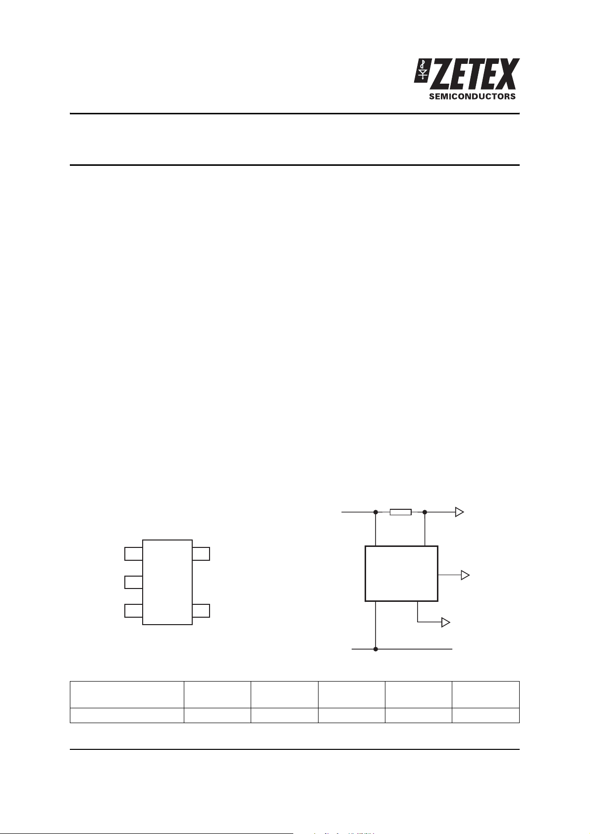
Typical application circuit
-
Pin connections
Flag
S-
R
V
+
IN
S+
S
54
S-
ZXCT1041
V
IN
Flag
1
GND
OUT
S+
GND
2
OUT
3
V
OUT
Ordering information
Order code Package Partmark Reel size
(inches)
ZXCT1041E5TA SOT23-5 1041 7 8 3000
Issue 2 - January 2008 1 www.zetex.com
© Zetex Semiconductors plc 2008
Tape width
(mm)
Quantity
per reel
Page 2
Absolute maximum ratings
ZXCT1041
Voltage on VS- and V
S+
Voltage on all other pins -0.6V to (V
V
[(VS+) - (VS-)] +/-6V
sense
Operating temperature, T
A
-0.6 to 20V
-40 to 125°C
or VS-) +0.6V
S+
Storage temperature -55 to 150°C
Maximum junction temperature, T
Package power dissipation 300mW at T
Operation above the absolute maximum rating may cause device failure. Operation at the absolute maximum ratings, for
extended periods, may reduce device reliability.
150°C
J
= 25°C (De-rate to zero at 150°C)
A
Recommended operating conditions
Parameter Min. Max. Units
V
S±
Flag Current direction flag output 0 V
V
SENSE
V
OUT
T
A
Common-mode sense input range 2.7 20 V
S±
V
Differential sense input voltage range 0 ±0.8 V
Output voltage range 0 VS± -1.5 V
Ambient temperature range -40 125 °C
Pin function table
Pin Name Description
1Flag
2 GND Ground pin
3 OUT Output voltage pin
4 S+ This is the positive input of the current monitor. It also acts as the supply
5 S- This is the negative input of the current monitor. The current through this
This is the current direction pin. It is open collector and allows the logic high
level to be set independent of V
voltage. Low indicates VS+ is greater than V
S+
voltage pin providing current for internal circuitry. The current through this
pin varies with differential sense voltage
pin varies with differential sense voltage
S-
Issue 2 - January 2008 2 www.zetex.com
© Zetex Semiconductors plc 2008
Page 3
Electrical characteristics
ZXCT1041
Test conditions TA = 25°C, VS+ = 10V, V
SENSE
= 100mV
Symbol Parameter Conditions Min. Typ. Max. Units
I
I
I
V
Q
S+
S-
OUT
Ground pin current 15 35 50 µA
VS+ input current V
VS- input current V
Output voltage
V
= 0V 10 17 24 µA
SENSE
= 0V 10 17 24 µA
SENSE
= +150mV 1.55 1.5 1.45 V
SENSE
[flag high]
= +100mV 1.02 1 0.98 V
SENSE
= +30mV 309 300 291 mV
SENSE
= 0V 0 15 mV
SENSE
= -30mV 285 300 315 mV
SENSE
= -100mV 0.95 1 1.05 V
SENSE
= -150mV 1.42 1.50 1.58 V
SENSE
= ±100mV 30 ppm/ºC
SENSE
V
OUT
TC V
[flag low] V
variation with
OUT
V
V
V
V
V
V
temperature
Gain V
OUT/VSENSE
10
Accuracy Total output error
V
= 100mV ±2 %
SENSE
(Gain + offset)
Accuracy Total output error
V
SENSE
= -100mV ±5 %
(Gain + offset)
BW Bandwidth V
CMRR V
common mode
S+
SENSE(DC)
V
SENSE(AC)
VIN = 2.7 to 20V 60 dB
= 100mV
= 63mV
300 kHz
PP
rejection ratio
Flag TP Flag trip point Referred to V
V
FL
Flag low output
I
= 100A60200mV
SINK
SENSE
-2.5 +2.5 mV
voltage
I
FH
Flag high leakage
VOH = 5V 1 A
current
NOTES:
(a) V
(b) Temperature dependent measurements are extracted from characterisation and simulation results.
= "VS+" - "VS-"
SENSE
Issue 2 - January 2008 3 www.zetex.com
© Zetex Semiconductors plc 2008
Page 4
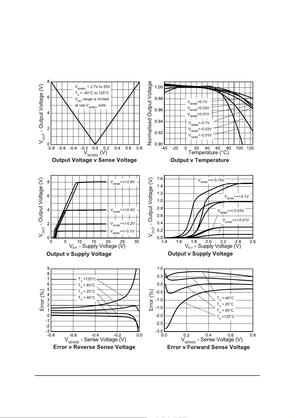
Typical characteristics
ZXCT1041
Conditions V
SENSE
+=10V, V
=100mV, TA=25°C unless otherwise stated.
SENSE
Issue 2 - January 2008 4 www.zetex.com
© Zetex Semiconductors plc 2008
Page 5

Typical characteristics
ZXCT1041
Conditions V
Sense+ Pin Current (µA)
+=10V, V
SENSE
8
6
4
Voltage (V)
2
0
-0.8 -0.6 -0.4 -0.2 0.0 0.2 0.4 0.6 0.8
V
OUT
700
600
500
400
300
200
100
0
-0.8 -0.6 -0.4 -0.2 0.0 0.2 0.4 0.6 0.8
I
SENSE+
FLAG VCC = 5V
R
= 50k
FLAG
V
& V
TA = -40°C to 125°C
v Sense Voltage
FLAG
V
v Sense Vo ltag e
=100mV, TA=25°C unless otherwise stated.
SENSE
(V)
SENSE
(V)
SENSE
300
250
(µA)
200
150
GND
100
50
FLAG VCC = 5V
4
(V) I
FLAG
V
700
600
500
400
300
200
100
Sense- Pin Current (µA)
R
= 50k
FLAG
2
0
-0.15 -0.10 -0.05 0.00 0.05 0.10 0.15
I
GND
0
-0.8 -0.6 -0.4 -0.2 0.0 0.2 0.4 0.6 0.8
I
SENSE-
V
& V
SENSE
v S e nse Voltage
FLAG
V
SENSE
v Sense Vo ltag e
Flag Current 100µA
(V)
TA = -40°C to 125°C
(V)
0
-5
-10
Gain Error (%)
-15
5
10
6
10
Output Load Resis tan ce (Ω)
Error v Resistive Loading
7
10
10
150
100
50
0
-50
-100
Output Voltage Error (mV)
-150
8
-10 -5 0 5 10
Output Load Curren t (µA))
Error v Current Load ing
Issue 2 - January 2008 5 www.zetex.com
© Zetex Semiconductors plc 2008
Page 6

Typical characteristics
ZXCT1041
Conditions V
Voltage (V)
Forward Large Signal Step Response
0.20
0.15
0.10
0.05
Voltage (V)
0.00
Forward Small Signal Step Re sp on se
+=10V, V
SENSE
2.0
1.5
1.0
0.5
0.0
-5 0 5 10 15 20 25 30
=100mV, TA=25°C unless otherwise stated.
SENSE
V
V
SENSE
Time (µs)
V
V
SENSE
-5 0 5 10 15 20 25 30 35
Time (µs)
2.0
1.5
OUT
1.0
0.5
Voltage (V)
0.0
-5 0 5 10 15 20 25 30
V
SENSE
V
OUT
Time (µs)
Reverse La rge Sign al Step Resp o n se
0.20
0.15
V
OUT
0.10
0.05
Voltage (V)
0.00
-5 0 5 10 15 20 25 30 35
V
SENSE
OUT
Time (µs)
Reverse Sm all Signal Step R esp o ns e
5
4
3
2
1
Voltage (V)
0
-1
-2
-4-20246810
V
FLAG
V
SENSE X10
Time (µs)
Large Sig Zero Crossing Response
2.0
1.5
1.0
V
OUT
Voltage (V)
0.5
0.0
-4 -2 0 2 4 6 8 10
Time (µs)
Large Sig Zero Crossing Response
Issue 2 - January 2008 6 www.zetex.com
© Zetex Semiconductors plc 2008
Page 7

Typical characteristics
ZXCT1041
Conditions V
Voltage (V)
Large Sig Zero Crossing Response
(V)
OUT
V
Small Sig Zero Crossing Resp on se
+=10V, V
SENSE
5
4
3
2
1
0
-1
-2
16 18 20 22 24 26 28 30
V
=100mV, TA=25°C unless otherwise stated.
SENSE
FLAG
V
SENSE X10
Time (µs)
5
4
3
2
1
0
-1
-2
-4 -2 0 2 4 6 8 10 12 14
V
V
SENSE X100
FLAG
Time (µs)
2.0
1.5
1.0
Voltage (V)
0.5
0.0
16 18 20 22 24 26 28 30
Time (us)
Large Sig Zero Crossing Response
0.20
0.15
(V)
0.10
OUT
V
0.05
0.00
-4 -2 0 2 4 6 8 10 12 14
Time (µs)
V
Small Sig Zero Crossing Resp on se
V
OUT
OUT
5
4
3
2
1
Vout (V)
0
-1
-2
16 18 20 22 24 26 28 30 32 34
V
V
SENSE X100
FLAG
Time (µs)
Small Sig Zero Crossing Response
0.20
0.15
0.10
V
OUT
Vout (V)
0.05
0.00
16 18 20 22 24 26 28 30 32 34
Time (µs)
Small Sig Zero Crossing Response
Issue 2 - January 2008 7 www.zetex.com
© Zetex Semiconductors plc 2008
Page 8

Typical characteristics
ZXCT1041
Conditions V
Reject i on (d B )
Gain (dB )
+=10V, V
SENSE
70
60
50
40
30
20
10
0
-10
100 1k 10k 100k 1M
Vs+=2.7V
Vs+=5.0V
Vs+=10V
Vs+=15V & 20V
=100mV, TA=25°C unless otherwise stated.
SENSE
V
=+100mVrms
SENSE
VAC=63mV
P-P
Frequency (Hz)
Forward CMRR
25
20
15
10
-10
-15
-20
-25
5
0
-5
V
=+100mV
SENSE
VAC=63mV
100k 1M
VS+=2.7V
VS+=5.0V
VS+=10V
VS+=15V
VS+=20V
P-P
Frequency (Hz)
Forward Frequency Response
70
60
50
40
30
20
10
Rejection (dB)
0
-10
100 1k 10k 100k 1M
Vs+=15V & 20V
Vs+=10V
Vs+=5.0V
Vs+=2.7V
V
=-100mVrms
SENSE
VAC=63mV
Frequency (Hz)
Reverse CMRR
25
20
15
10
5
0
-5
-10
V
Gain (dB)
-15
-20
-25
=-100mV
SENSE
VAC=63mV
100k 1M
VS+=2.7V
VS+=5.0V
VS+=10V
VS+=15V
VS+=20V
P-P
Frequency (Hz)
Reverse Frequency Response
P-P
Issue 2 - January 2008 8 www.zetex.com
© Zetex Semiconductors plc 2008
Page 9

ZXCT1041
Application information
The ZXCT1041 uses two current monitors in anti-parallel to provide bidirectional current
measurement. The integrated resistors while having a broad actual value variance provide very
good matching to one another; this provides very tight gain matching from forward current
measurement to reverse current management and removes the need to trim the resistor values.
The internal transconductance setting resistors have a nominal value of 1.5k⍀ thereby setting the
internal transconductance to 0.67mA/V of V
are summed into an internal common gain-setting resistor of 15k⍀. This sets the overall gain to
10 which has a very small variance due to the very good matching of internal transistors.
To improve accuracy the offset of amplifier 1 is trimmed.
The direction of measured current flow is determined by comparing the voltages applied to the
bases of transconductance transistors (Q1 and Q2). For maximum versatility the flag output uses
an open collector; this allows the ZXCT1041 to monitor rails at a much higher potential than what
the flag output is interfacing to.
S+ S-
. The outputs of both current monitors (current)
SENSE-
1.5k 1.5k
OUT
Flag
15k
GND
A common application for micro-power current monitors is measuring the discharge current of a
rechargeable lithium ion/polymer battery. The ZXCT1041 enables measuring both the charge and
discharge current into the battery and with its wide operating voltage of 2.5 to 20V enables it to
measure the currents in to/ out of up to 4 cells connected in series.
Issue 2 - January 2008 9 www.zetex.com
© Zetex Semiconductors plc 2008
Page 10

ZXCT1041
Load
Battery
charger
control
When choosing appropriate values for R
S-
ZXCT1041
GND
a compromise must be reached between in-line
SENSE
S+
Battery
Flag
OUT
signal loss (including potential power dissipation effects) and small signal accuracy.
Higher values for R
gives better accuracy at low load currents by reducing the inaccuracies
SENSE
due to internal offsets. For best operation the ZXCT1041 has been designed to operate with
V
of the order of 50mV to 150mV.
SENSE
Issue 2 - January 2008 10 www.zetex.com
© Zetex Semiconductors plc 2008
Page 11

Package outline - SOT23-5
DIM Millimeters Inches
Min. Max. Min. Max.
A 0.90 1.45 0.0354 0.0570
A1 0.00 0.15 0.00 0.0059
A2 0.90 1.30 0.0354 0.0511
b 0.20 0.50 0.0078 0.0196
C 0.09 0.26 0.0035 0.0102
D 2.70 3.10 0.1062 0.1220
E 2.20 3.20 0.0866 0.1181
E1 1.30 1.80 0.0511 0.0708
e 0.95 REF 0.0374 REF
e1 1.90 REF 0.0748 REF
L 0.10 0.60 0.0039 0.0236
a° 0° 30° 0° 30°
Note: Controlling dimensions are in millimeters. Approximate dimensions are provided in inches
ZXCT1041
Issue 2 - January 2008 11 www.zetex.com
© Zetex Semiconductors plc 2008
Page 12

ZXCT1041
Definitions
Product change
Zetex Semiconductors reserves the right to alter, without notice, specifications, design, price or conditions of supply of any product or
service. Customers are solely responsible for obtaining the latest relevant information before placing orders.
Applications disclaimer
The circuits in this design/application note are offered as design ideas. It is the responsibility of the user to ensure that the circuit is fit for
the user’s application and meets with the user’s requirements. No representation or warranty is given and no liability whatsoever is
assumed by Zetex with respect to the accuracy or use of such information, or infringement of patents or other intellectual property rights
arising from such use or otherwise. Zetex does not assume any legal responsibility or will not be held legally liable (whether in contract,
tort (including negligence), breach of statutory duty, restriction or otherwise) for any damages, loss of profit, business, contract,
opportunity or consequential loss in the use of these circuit applications, under any circumstances.
Life support
Zetex products are specifically not authorized for use as critical components in life support devices or systems without the express written
approval of the Chief Executive Officer of Zetex Semiconductors plc. As used herein:
A. Life support devices or systems are devices or systems which:
1. are intended to implant into the body
or
2. support or sustain life and whose failure to perform when properly used in accordance with instructions for use provided in the
labelling can be reasonably expected to result in significant injury to the user.
B. A critical component is any component in a life support device or system whose failure to perform can be reasonably expected to
cause the failure of the life support device or to affect its safety or effectiveness.
Reproduction
The product specifications contained in this publication are issued to provide outline information only which (unless agreed by the
company in writing) may not be used, applied or reproduced for any purpose or form part of any order or contract or be regarded as a
representation relating to the products or services concerned.
Terms and Conditions
All products are sold subjects to Zetex’ terms and conditions of sale, and this disclaimer (save in the event of a conflict between the two
when the terms of the contract shall prevail) according to region, supplied at the time of order acknowledgement.
For the latest information on technology, delivery terms and conditions and prices, please contact your nearest Zetex sales office.
Quality of product
Zetex is an ISO 9001 and TS16949 certified semiconductor manufacturer.
To ensure quality of service and products we strongly advise the purchase of parts directly from Zetex Semiconductors or one of our
regionally authorized distributors. For a complete listing of authorized distributors please visit: www.zetex.com/salesnetwork
Zetex Semiconductors does not warrant or accept any liability whatsoever in respect of any parts purchased through unauthorized sales channels.
ESD (Electrostatic discharge)
Semiconductor devices are susceptible to damage by ESD. Suitable precautions should be taken when handling and transporting devices.
The possible damage to devices depends on the circumstances of the handling and transporting, and the nature of the device. The extent
of damage can vary from immediate functional or parametric malfunction to degradation of function or performance in use over time.
Devices suspected of being affected should be replaced.
Green compliance
Zetex Semiconductors is committed to environmental excellence in all aspects of its operations which includes meeting or exceeding
regulatory requirements with respect to the use of hazardous substances. Numerous successful programs have been implemented to
reduce the use of hazardous substances and/or emissions.
All Zetex components are compliant with the RoHS directive, and through this it is supporting its customers in their compliance with
WEEE and ELV directives.
Product status key:
“Preview” Future device intended for production at some point. Samples may be available
“Active” Product status recommended for new designs
“Last time buy (LTB)” Device will be discontinued and last time buy period and delivery is in effect
“Not recommended for new designs”
“Obsolete” Production has been discontinued
Datasheet status key:
“Draft version” This term denotes a very early datasheet version and contains highly provisional information, which
“Provisional version” This term denotes a pre-release datasheet. It provides a clear indication of anticipated performance.
“Issue” This term denotes an issued datasheet containing finalized specifications. However, changes to
Zetex sales offices
Europe
Zetex GmbH
Kustermann-park
Balanstraße 59
D-81541 München
Germany
Telefon: (49) 89 45 49 49 0
Fax: (49) 89 45 49 49 49
europe.sales@zetex.com
© 2008 Published by Zetex Semiconductors plc
Device is still in production to support existing designs and production
may change in any manner without notice.
However, changes to the test conditions and specifications may occur, at any time and without notice.
specifications may occur, at any time and without notice.
Americas
Zetex Inc
700 Veterans Memorial Highway
Hauppauge, NY 11788
USA
Telephone: (1) 631 360 2222
Fax: (1) 631 360 8222
usa.sales@zetex.com
Asia Pacific
Zetex (Asia Ltd)
3701-04 Metroplaza Tower 1
Hing Fong Road, Kwai Fong
Hong Kong
Telephone: (852) 26100 611
Fax: (852) 24250 494
asia.sales@zetex.com
Corporate Headquarters
Zetex Semiconductors plc
Zetex Technology Park, Chadderton
Oldham, OL9 9LL
United Kingdom
Telephone: (44) 161 622 4444
Fax: (44) 161 622 4446
hq@zetex.com
Issue 2 - January 2008 12 www.zetex.com
© Zetex Semiconductors plc 2008
 Loading...