

Page 1
A
Product Line o
f
Diodes Incorporated
ZXCT1030
HIGH-SIDE CURRENT MONITOR WITH COMPARATOR
Description
The ZXCT1030 is a high side current sense monitor
containing an internal reference and comparator with a nonlatching output. Using this device eliminates the need to
disrupt the ground plane when sensing a load current.
The wide input voltage range of 20V do wn to as low as 2.2V
make it suitable for a range of applications. Dynamics and
supply current are optimized for the processing of fast pulses,
associated with switch mode applications
.
Features
• Low cost, accurate high-side current sensing
• Output voltage scaling
• Up to 18V output
• 2.2V - 20V supply range
• Voltage reference on chip
• Comparator on chip
• SO8 package
Pin Assignments
V
CC
V
SENSE-
V
SENSE+
GND
Applications
• Battery chargers
• Electronic fuse
• DC motor control
• Over current monitor
• Power management
• Inrush current limiting
V
COMP_OUT
V
OUT
Vref_out
V
COMP_IN
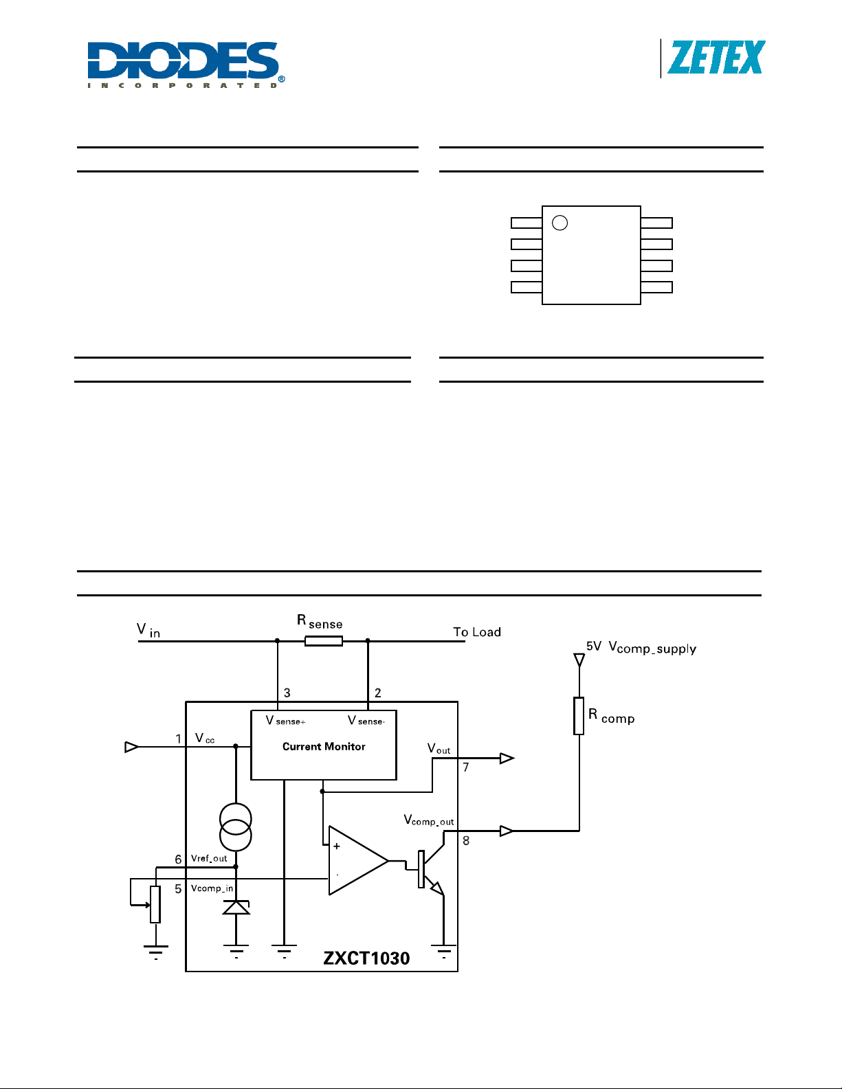
Typical Application Circuit
ZXCT1030
Document number: DS32161 Rev. 4 - 2
1 of 7
www.diodes.com
June 2010
© Diodes Incorporated
Page 2

A
f
Pin Description
Pin Name Function
VCC
V
SENSE-
V
SENSE+
GND
V
COMP_IN
V
REF_OUT
V
OUT
V
COMP_OUT
Supply voltage
Negative sense input
Positive sense input
Ground
Comparator input, usually a ratio of the
reference or other control signal
Reference output
Current monitor output voltage
Open collector comparator output
Product Line o
Diodes Incorporated
ZXCT1030
Absolute Maximum Ratings
Parameter Rating Unit
Voltage on any pin
-0.6 and VCC +0.6
V
Operating Temperature -40 to 85 °C
Storage Temperature -55 to 125 °C
Package Power Dissipation
(T
AMB
= 25)
°C
SO8 700 mW
Recommended Operating Conditions
Parameter Min Max Units
VCC
V
V
V
V
T
SENSE+
(a)
SENSE
OUT
COMP_IN
AMB
ZXCT1030
Document number: DS32161 Rev. 4 - 2
2.2 20 V
2.2
VCC
V
10 500 mV
0
V
SENSE-
-1V
V
0.005 10 V
-40 85 °C
2 of 7
www.diodes.com
June 2010
© Diodes Incorporated
Page 3
A
Product Line o
f
V
V
V
V
V
V
V
V
V
V
V
V
V
T
V
V
V
V
V
V
V
V
V
V
A
A
V
V
V
V
V
V
V
T
V
w
V
Y
V
V
V
T
Diodes Incorporated
ZXCT1030
Electrical Characteristics (ZXCT1030N8) – Test conditions T
V
COMP_SUPPLY
= 5V unless otherwise stated.
= 25°C, VIN = VCC = 15V, R
AMB
COMP
= 10kΩ,
Symbol Parameter Condition Min. Typ. Max. Unit
CC
SENSE
OUT
R
OUT
OUT
C
ICC
I
SENSE
I
SENSE
CM(MIN)
CC
GAIN
+
+
-
(B)
Range
CC
Sense+ Range 2.2
Output Voltage
Output Resistance
OUT
Temperature Coefficient
Supply Current
+ Input Current
SENSE
- Input Current
SENSE
Minimum Active Common Mode Voltage
ccuracy
OUT/VSENSE
BW Bandwidth
= 0
SENSE
= 10
SENSE
= 30
SENSE
= 50
SENSE
= 100
SENSE
= 500
SENSE
= 15V,
SENSE -
= 1V
OUT
= 15V
SENSE -
= 14.9V
SENSE-
= 15V
CC
COMP_SUPPLY =
COMP_IN
SENSE
SENSE
SENSE
SENSE
SENSE
= V
REF
= 10mV
= 100mV
= 100mV
= 10mVp-p
= 100mVp-p
5V
2.2 20 V
mV
0
88
284
480
970
4500
2
100
300
500
1000
5000
VCC
10
112
316
520
1030
5500
1.2 1.5 1.8 kΩ
30 ppm/°C
170 270 350 µA
48 90 µA
70 220 nA
2.8 V
-3 3 %
9.7 10.0 10.3
3
6
MHz
COMPARATOR
Input Voltage 0.005 10 V
COMP_IN
H
IB
D
OL
OH
IOL
IOH
Hysteresis 15 mV
Input Bias 5 80 150 nA
Propagation Delay 100 ns
Output Voltage Lo
Output Voltage High
Output Sink Current
30 150 200 mV
V
COMP_
SUPPL
ol = 0.4V 2 mA
Output High Leakage Current 1.0 µA
oltage Reference
REF
Delta V
C
Change in V
REF
REF
Reference Current =
+300µA to -5µA
SOURCE
300µA
SINK
5µA to
I
I
1.200 1.240 1.280 V
10 mV
30 ppm/°C
PSR Supply Rejection 0.01 %/V
Notes: (a) (V
(b) Level of V
ZXCT1030
Document number: DS32161 Rev. 4 - 2
SENSE+
) – (V
-)
SENSE
+ where comparator output defaults to ‘off’.
SENSE
www.diodes.com
3 of 7
June 2010
© Diodes Incorporated
Page 4

A
f
Typical Application Circuits
Product Line o
Diodes Incorporated
ZXCT1030
ZXCT1030
Document number: DS32161 Rev. 4 - 2
4 of 7
www.diodes.com
June 2010
© Diodes Incorporated
Page 5

A
Product Line o
f
Diodes Incorporated
ZXCT1030
Voltage output current monitor
Referring to the block diagram, the current monitor takes the small volt age developed across the sense resistor (V
and transfers it from the large common mode supply voltage to a ground referenced signal with a gain of 10. The sense
input common mode range is 2.2V to 20V. In this range, a linear output voltage is delivered.
SENSE
)
Reference
The bandgap reference allows the comparator to compar e the translated V
which can be any voltage from 0 to 1.24V, configured by two external resistors which forms V
The output current which can be drawn from the comparator reference (I
potentiometers ≥250kΩ suitable for setting a threshold level. Where a lower potentiometer resistor value is used, an
additional resistor value should be inserted between V
and VCC to maintain sufficient current for the reference.
REF
(as shown in Figure 1).
Figure 1: External Resistor for Reference Level
The voltage reference has a maximum current sink capab ility. This magnitude of current will be influenced by the value of
R1 which is inserted between V
and VCC. The value of current flowing through R1 can be expressed as:
REF
I = (V
CC
-V
REF
) / R1
with threshold value chosen by the user
SENSE
COMP_IN
source) is limited to 5μA, making
REF
.
Comparator
The open collector output is active low and is asserted when V
voltage rail up to V
via a pull-up resistor. Suggest values for the resistor are in the range of 10-100kΩ.
IN
In the case where high load currents or a short circuit occurs, thus reducing the common mode si gnals (V+, V-) typically
below 2.2V, the comparator will default to the asserted state. This can eliminate a closed l oop system 'latch-up' condition,
allowing the controller to remove the applied power.
Stability
To ensure stable operation of the ZXCT1030, it is recommended a decoupling capacitor is placed across the VCC and
ground connections. A ceramic 10µF will be adequate.
ZXCT1030
Document number: DS32161 Rev. 4 - 2
5 of 7
www.diodes.com
SENSE
x 10 (V
OUT
) > V
COMP_IN
. It can be connected to any
June 2010
© Diodes Incorporated
Page 6

A
f
Ordering Information*
Product Line o
Diodes Incorporated
ZXCT1030
Device Status(*) Package
Marking
Device
Reel Size
(inches)
Tape Width
(mm)
Quantity
Per reel
ZXCT1030X8TA Obsolete MSOP8 ZXCT1030 7 12 1000
ZXCT1030N8TA Active SO8 ZXCT1030 7 12 500
Notes: *ZXCT1030X8TA is obsolete for more device information please check our obsolete products search on diodes website
Package Outline – SO8
ZXCT1030
Document number: DS32161 Rev. 4 - 2
6 of 7
www.diodes.com
June 2010
© Diodes Incorporated
Page 7

A
Product Line o
f
Diodes Incorporated
ZXCT1030
DIODES INCORPORATED MAKES NO WARRANTY OF ANY KIND, EXPRESS OR IMPLIED, WITH REGARDS TO THIS DOCUMENT,
INCLUDING, BUT NOT LIMITED TO, THE IMPLIED WARRANTIES OF MERCHANTABILITY AND FITNESS FOR A PARTICULAR
PURPOSE (AND THEIR EQUIVALENTS UNDER THE LAWS OF ANY JURISDICTION).
Diodes Incorporated and its subsidiaries reserve the right to make modifications, enhancements, improvements, corrections or other changes
without further notice to this document and any product described herein. Diodes Incorporated does not assume any liability arising out of the
application or use of this document or any product described herein; neither does Diodes Incorporated convey any license under its patent or
trademark rights, nor the rights of others. Any Customer or user of this document or products des cribed herein in such applications shall
assume all risks of such use and will agree to hold Diodes Incorporated and all the companies whose products are represented on Diodes
Incorporated website, harmless against all damages.
Diodes Incorporated does not warrant or accept any liability whatsoever in respect of any products purchased through unauthorized sales
channel.
Should Customers purchase or use Diodes Incorporated products for any unintended or unauthorized application, Customers shall indemnify
and hold Diodes Incorporated and its representatives harmless against all claims, damages, expenses, and attorney fees arising out of,
directly or indirectly, any claim of personal injury or death associated with such unintended or unauthorized application.
Products described herein may be covered by one or more United States, international or foreign patents pending. Product names and
markings noted herein may also be covered by one or more United States, international or foreign trademarks.
Diodes Incorporated products are specifically not authorized for use as critical components in life support devices or systems without the
express written approval of the Chief Executive Officer of Diodes Incorporated. As used herein:
A. Life support devices or systems are devices or systems which:
1. are intended to implant into the body, or
2. support or sustain life and whose failure to perform when properly used in accordance with instructions for use provided in the
labeling can be reasonably expected to result in significant injury to the user.
B. A critical component is any component in a life support device or system whose failure to perform can be reasonably expected to cause
the failure of the life support device or to affect its safety or effectiveness.
Customers represent that they have all necessary expertise in the safety and regulatory ramifications of their life support devices or systems,
and acknowledge and agree that they are solely responsible for all legal, regulatory and safety-related requirements concerning their products
and any use of Diodes Incorporated products in such safety-critical, life support devices or systems, notwithstanding any devices- or systemsrelated information or support that may be provided by Diodes Incorporated. Further, Customers must fully indemnify Diodes Incorporated and
its representatives against any damages arising out of the use of Diodes Incorporated products in such safety-critical, life support devices or
systems.
Copyright © 2010, Diodes Incorporated
IMPORTANT NOTICE
LIFE SUPPORT
www.diodes.com
ZXCT1030
Document number: DS32161 Rev. 4 - 2
7 of 7
www.diodes.com
June 2010
© Diodes Incorporated
 Loading...