

Page 1
ZXCT1020
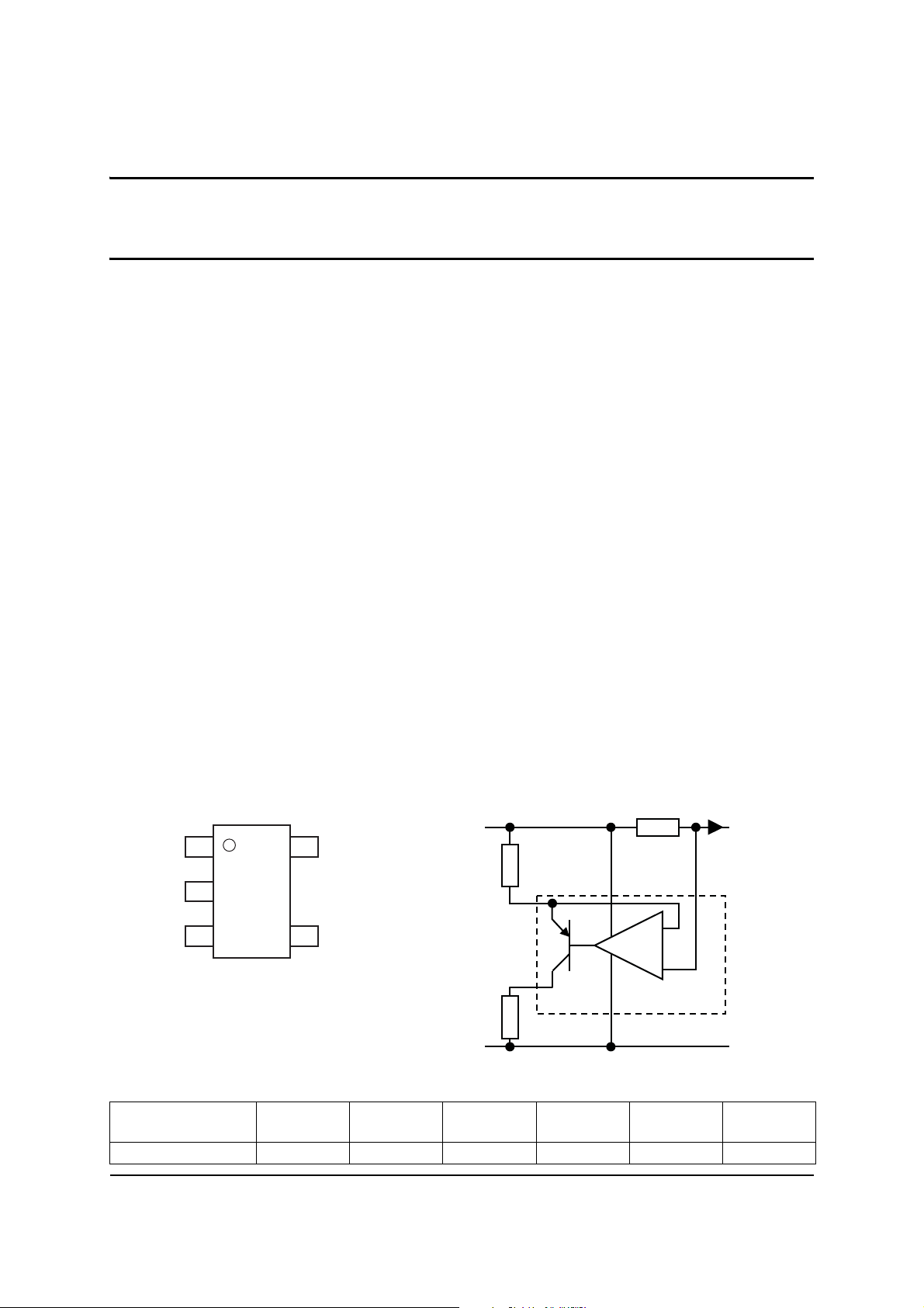
S+
GND
OUT
S-
V
B
Top view
1
2
3
5
4
Low offset current output current monitor
Description
The ZXCT1020 is a precision high-side current
sense monitor. Using this type of device
eliminates the need to disrupt the ground
plane when sensing a load current.
The ZXCT1020 uses two external resistors to
set the overall voltage gain for applications
where improved accuracy at small sense
voltages is required. For fixed gain variants
Zetex offers the ZXCT1021 (G=10) and
ZXCT1022 (G=100).
The ZXCT1020 footprint follows that of the
ZXCT1021/2 with only 2 additional resistors
required:
One resistor between pins 1 and 4 for setting
transconductance, and the other between
pins 3 and 2 for setting overall gain.
Current output enables the user to set the gain
via these external resistors. Using two external
resistors to set the gain ensures optimal
versatility as the transconductance can be varied
to meet the output impedance requirements of
the load that the ZXCT1020 has to drive.
The very low offset voltage enables a typical
accuracy of 3% for sense voltages of only 10mV,
giving better tolerances for small sense
resistors necessary at higher currents.
The wide input voltage range of 20V down to as
low as 2.5V make it suitable for a range of
applications. With a minimum operating current
of just 25µA, combined with its SOT23-5
package make it suitable for portable battery
equipment too.
ZXCT1020
Features
• Accurate high-side current sensing
• Versatile current output scaling
• 2.5V - 20V operating range
• 25µA quiescent current
• 1% typical accuracy
• SOT23-5 package
Applications
• Battery chargers
• Over-current monitor
• Motherboard power supply current measurement
• Level translating
• Programmable current source
Pinout information Typical application circuit
R
S
R
SH
S+
V
B
1
4
-
+
V
OUT
R
G
3
ZXCT1020
2
GND
I
L
S(LOAD)
5
Ordering information
Order reference Package Device
marking
ZXCT1020E5TA SOT23-5 1020 Preview 7 3000 8
Issue 1 - August 2007 1 www.zetex.com
© Zetex Semiconductors plc 2007
Status Reel size
(inches)
Quantity
per reel
Tape width
(mm)
Page 2
ZXCT1020
NOTES:
Absolute maximum ratings
Voltage on VB with respect to GND pin -0.5V to 20V
(a)
Voltage on S+
SENSE
(c)
V
(b)
, S-
, OUT with respect to GND pin
Junction temperature -40°C to125°C
Storage temperature -55°C to 150°C
Package power dissipation (T
NOTES:
(a) Subject to V
(b) Subject to absolute maximum V
(c) V
(d) V
is defined as the voltage difference across the sense resistor. and is the voltage across resistor RSH plus the
SENSE
voltage between S+ and S-.
might need to be reduced when used with smaller values of RSH and at larger rails due to increased power dissipation.
SENSE
+ never going 6V below VB.
SENSE
= 25°C) SOT23-5 300mW
amb
not being exceeded.
SENSE
Pin out information
Pin Name Pin function
1 S+ Positive sense input. Should be tied to positive side of sense resistor via
resistance (R
2 GND Ground and substrate connection of device.
3 OUT Current output. A gain setting resistor (R
connected to this pin to set overall voltage gain of:
Gain = R
The resistance, RG, placed on out will set the ZXCT1020 output impedance equal
. When driving low impedance loads both RG and RSH should be reduced.
to R
G
4V
B
Input voltage pin. Provides bias to current monitor and should be tied to the
rail whose current is being monitored.
5 S- High impedance negative sense voltage input
) of the order of 150⍀ to 1.5k⍀.
SH
G/RSH
) referenced to GND should be
G
-0.5V to V
+0.5V
B
-0.5V to +2.5V
(d)
Recommended operating conditions
Parameter Min. Max. Units
V
SENSE+
V
B
V
SENSE
V
OUT
R
SH
T
A
(*) For best performance VB and V
Common-mode sense input range 2.5 20 V
Bias pin input voltage range
(*)
2.5 20 V
Differential sense Input voltage range 0 1.5 V
Output voltage range 0 V
SENSE-
- 1 V
Shunt resistor value 120 2000 ⍀
Ambient temperature range -40 85 °C
should be referred to the rail whose current is being measured.
SENSE+
Recommended resistor gain setting combinations
Gain R
SHUNT
10 1.5k⍀ 15k⍀
20 750⍀ 15k⍀
50 300⍀ 15k⍀
100 150⍀ 15k⍀
Issue 1 - August 2007 2 www.zetex.com
© Zetex Semiconductors plc 2007
R
GAIN
Page 3
ZXCT1020
Electrical characteristics
T
= 25°C, V
amb
SENSE+
Symbol Parameter Conditions Limits Unit
V
OUT
Output voltage V
TC[1] Output voltage temperature
coefficient
I
Q
I
S-
I
+ S+ input current V
S
Ground pin current V
S- input current V
Acc Accuracy V
Gain V
R
OUT
OUT
Output resistance RG not connected 370 M⍀
BW Bandwidth V
PSRR Power supply rejection ratio V
= VB = 15V, V
/V
SENSE
= 100mV, RG = 15k⍀, RSH = 1.5k⍀ unless otherwise stated.
SENSE
Min. Typ. Max.
= 0mV 3 15 mV
SENSE
V
V
V
= 30mV 291 300 309 mV
SENSE
= 100mV 0.98 1 1.02 V
SENSE
= 150mV 1.47 1.5 1.53 V
SENSE
50 300 ppm
= 0V 25 35 A
SENSE
= 0V 20 100 nA
SENSE
= 0V 100 nA
SENSE
= 100mV -2 2 %
SENSE
V
V
= 100mV 10 V/V
SENSE
(DC) = 10mV 300 kHz
SENSE
(DC) = 100mV 2 MHz
SENSE
SENSE+
= VB = 2.5 to 20V 70 80 dB
Issue 1 - August 2007 3 www.zetex.com
© Zetex Semiconductors plc 2007
Page 4
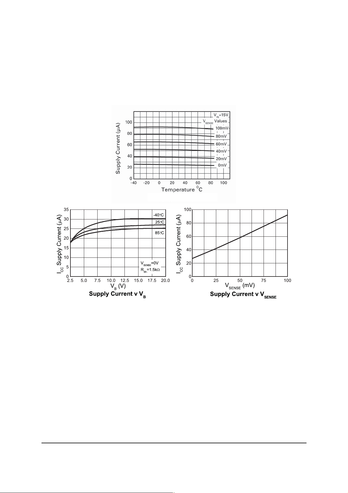
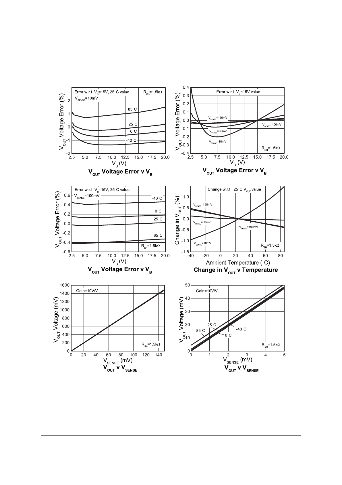
Typical characteristics
ZXCT1020
Test conditions unless otherwise stated: TA = 25°C, VB = V
R
= 1.5k⍀, RG = 15k⍀.
SH
Supply current v Temperature
SENSE+
(via RSH) =15V, V
SENSE
= 100mV
Issue 1 - August 2007 4 www.zetex.com
© Zetex Semiconductors plc 2007
Page 5
ZXCT1020
°
°
°
°
°
°
°
°
°
°
°
°
°
°
°
Test conditions unless otherwise stated: TA = 25°C, VB = V
Gain = 10, R
= 15k⍀.
G
SENSE+
(via RSH) =15V, V
SENSE
= 100mV
Issue 1 - August 2007 5 www.zetex.com
© Zetex Semiconductors plc 2007
Page 6

ZXCT1020
Test conditions unless otherwise stated: TA = 25°C, VB = V
Gain = 20, R
= 15k⍀.
G
°
°
°
°
°
SENSE+
°
(via RSH) =15V, V
°
°
SENSE
= 100mV
°
°
°
°
°
°
°
°
Issue 1 - August 2007 6 www.zetex.com
© Zetex Semiconductors plc 2007
Page 7

ZXCT1020
°
°
°
°
°
°
°
V
SENSE
= 10mV
Gain = 100
Test conditions unless otherwise stated: TA = 25°C, VB = V
R
= 15k⍀.
G
SENSE+
(via RSH) =15V, V
SENSE
= 100mV
Issue 1 - August 2007 7 www.zetex.com
© Zetex Semiconductors plc 2007
Page 8

Typical AC characteristics
Gain = 10
Gain = 50
Test conditions unless otherwise stated: TA = 25°C, VB = V
R
= 15k⍀.
G
SENSE+
ZXCT1020
(via RSH) =15V, V
SENSE
= 100mV,
Issue 1 - August 2007 8 www.zetex.com
© Zetex Semiconductors plc 2007
Page 9

ZXCT1020
Various gains with constant R
G
Test conditions unless otherwise stated: TA = 25°C, RG=15k, VB = V
V
= 100mV unless otherwise stated.
SENSE
SENSE+
(via RSH) =15V,
Issue 1 - August 2007 9 www.zetex.com
© Zetex Semiconductors plc 2007
Page 10

ZXCT1020
Test conditions unless otherwise stated: TA = 25°C, G=100, RG = 15k, VB = V
V
SENSE
= 100mV.
SENSE+
(via RSH),
Issue 1 - August 2007 10 www.zetex.com
© Zetex Semiconductors plc 2007
Page 11

ZXCT1020
V
OUT
R
G
R
SH
----------
V
SENSE
×=
Application information
The ZXCT1020 has a VB pin that is used to provide power to the current monitor. The maximum
voltage applied to the ZXCT1020 must be applied to this pin. The S+ and S- pins are used to
measure the current flowing to the load through the sense resistor. In normal use, the S+ is tied
to V
via a shunt resistor, RH making the ZXCT1020 essentially line powered.
B
The ZXCT1020 has a programmable gain set by the ratio of two external resistors R
I
L
S(LOAD)
R
SH
V
R
S
B
and RSH.
G
S+
1
4
5
-
+
V
OUT
R
G
sets the transconductance whereas RG set the gain and results in an output voltage defined
R
SH
as:
Where V
The ZXCT1020 has been tested to the same conditions as the ZXCT1021 giving an overall voltage
gain of 10. The gain of the ZXCT1020 can be adjusted simply by varying R
of 50 R
Decreasing R
reduce the overall output impedance.
is increased from 15k⍀ to 75k⍀. An alternative is to decrease RSH from 1.5k⍀ to 300⍀.
G
SH
= R
SENSE
increases the transconductance and, if for any given gain, reducing the RSH will
SENSE
x I
3
ZXCT1020
2
GND
L
. So to achieve a gain
G
To achieve a gain of 100, for example, the following resistor values could be used:
R
= 150 RG = 15k
SH
Issue 1 - August 2007 11 www.zetex.com
© Zetex Semiconductors plc 2007
Page 12

ZXCT1020
Intentionally left blank
Issue 1 - August 2007 12 www.zetex.com
© Zetex Semiconductors plc 2007
Page 13

Package outline - SOT23-5
Dim. Millimeters Inches
Min. Max. Min. Max.
A 0.90 1.45 0.0354 0.0570
A1 0.00 0.15 0.00 0.0059
A2 0.90 1.30 0.0354 0.0511
b 0.20 0.50 0.0078 0.0196
C 0.09 0.26 0.0035 0.0102
D 2.70 3.10 0.1062 0.1220
E 2.20 3.20 0.0866 0.1181
E1 1.30 1.80 0.0511 0.0708
e 0.95 REF 0.0374 REF
e1 1.90 REF 0.0748 REF
L 0.10 0.60 0.0039 0.0236
a° 0° 30° 0° 30°
Note: Controlling dimensions are in millimeters. Approximate dimensions are provided in inches
ZXCT1020
Issue 1 - August 2007 13 www.zetex.com
© Zetex Semiconductors plc 2007
Page 14

ZXCT1020
Definitions
Product change
Zetex Semiconductors reserves the right to alter, without notice, specifications, design, price or conditions of supply of any product or
service. Customers are solely responsible for obtaining the latest relevant information before placing orders.
Applications disclaimer
The circuits in this design/application note are offered as design ideas. It is the responsibility of the user to ensure that the circuit is fit for
the user’s application and meets with the user’s requirements. No representation or warranty is given and no liability whatsoever is
assumed by Zetex with respect to the accuracy or use of such information, or infringement of patents or other intellectual property rights
arising from such use or otherwise. Zetex does not assume any legal responsibility or will not be held legally liable (whether in contract,
tort (including negligence), breach of statutory duty, restriction or otherwise) for any damages, loss of profit, business, contract,
opportunity or consequential loss in the use of these circuit applications, under any circumstances.
Life support
Zetex products are specifically not authorized for use as critical components in life support devices or systems without the express written
approval of the Chief Executive Officer of Zetex Semiconductors plc. As used herein:
A. Life support devices or systems are devices or systems which:
1. are intended to implant into the body
or
2. support or sustain life and whose failure to perform when properly used in accordance with instructions for use provided in the
labelling can be reasonably expected to result in significant injury to the user.
B. A critical component is any component in a life support device or system whose failure to perform can be reasonably expected to
cause the failure of the life support device or to affect its safety or effectiveness.
Reproduction
The product specifications contained in this publication are issued to provide outline information only which (unless agreed by the
company in writing) may not be used, applied or reproduced for any purpose or form part of any order or contract or be regarded as a
representation relating to the products or services concerned.
Terms and Conditions
All products are sold subjects to Zetex’ terms and conditions of sale, and this disclaimer (save in the event of a conflict between the two
when the terms of the contract shall prevail) according to region, supplied at the time of order acknowledgement.
For the latest information on technology, delivery terms and conditions and prices, please contact your nearest Zetex sales office.
Quality of product
Zetex is an ISO 9001 and TS16949 certified semiconductor manufacturer.
To ensure quality of service and products we strongly advise the purchase of parts directly from Zetex Semiconductors or one of our
regionally authorized distributors. For a complete listing of authorized distributors please visit: www.zetex.com/salesnetwork
Zetex Semiconductors does not warrant or accept any liability whatsoever in respect of any parts purchased through unauthorized sales channels.
ESD (Electrostatic discharge)
Semiconductor devices are susceptible to damage by ESD. Suitable precautions should be taken when handling and transporting devices.
The possible damage to devices depends on the circumstances of the handling and transporting, and the nature of the device. The extent
of damage can vary from immediate functional or parametric malfunction to degradation of function or performance in use over time.
Devices suspected of being affected should be replaced.
Green compliance
Zetex Semiconductors is committed to environmental excellence in all aspects of its operations which includes meeting or exceeding
regulatory requirements with respect to the use of hazardous substances. Numerous successful programs have been implemented to
reduce the use of hazardous substances and/or emissions.
All Zetex components are compliant with the RoHS directive, and through this it is supporting its customers in their compliance with
WEEE and ELV directives.
Product status key:
“Preview” Future device intended for production at some point. Samples may be available
“Active” Product status recommended for new designs
“Last time buy (LTB)” Device will be discontinued and last time buy period and delivery is in effect
“Not recommended for new designs”
“Obsolete” Production has been discontinued
Datasheet status key:
“Draft version” This term denotes a very early datasheet version and contains highly provisional information, which
“Provisional version” This term denotes a pre-release datasheet. It provides a clear indication of anticipated performance.
“Issue” This term denotes an issued datasheet containing finalized specifications. However, changes to
Zetex sales offices
Europe
Zetex GmbH
Kustermannpark
Balanstraße 59
D-81541 München
Germany
Telefon: (49) 89 45 49 49 0
Fax: (49) 89 45 49 49 49
europe.sales@zetex.com
© 2007 Published by Zetex Semiconductors plc
Device is still in production to support existing designs and production
may change in any manner without notice.
However, changes to the test conditions and specifications may occur, at any time and without notice.
specifications may occur, at any time and without notice.
Americas
Zetex Inc
700 Veterans Memorial Highway
Hauppauge, NY 11788
USA
Telephone: (1) 631 360 2222
Fax: (1) 631 360 8222
usa.sales@zetex.com
Asia Pacific
Zetex (Asia Ltd)
3701-04 Metroplaza Tower 1
Hing Fong Road, Kwai Fong
Hong Kong
Telephone: (852) 26100 611
Fax: (852) 24250 494
asia.sales@zetex.com
Corporate Headquarters
Zetex Semiconductors plc
Zetex Technology Park, Chadderton
Oldham, OL9 9LL
United Kingdom
Telephone: (44) 161 622 4444
Fax: (44) 161 622 4446
hq@zetex.com
Issue 1 - August 2007 14 www.zetex.com
© Zetex Semiconductors plc 2007
 Loading...